Method of fabricating a distributed bragg reflector having enhanced thermal and electrical properties

a distributed bragg reflector and thermal and electrical properties technology, applied in the direction of lasers, optical resonator shape and construction, semiconductor lasers, etc., can solve the problems of telecommunications-important wavelength of 1.55 .mu.m., the accuracy and reproducibility of as is difficult to achieve in dbr fabrication, and the sb composition of algaassb semiconductor systems is difficult to achieve. , to achieve the effect of enhancing the thermal and reflectiv

Inactive Publication Date: 2002-02-28
RGT UNIV OF CALIFORNIA
View PDF0 Cites 2 Cited by
  • Summary
  • Abstract
  • Description
  • Claims
  • Application Information

AI Technical Summary

Benefits of technology

0015] Accordingly, one object of the present invention is to provide a method of controlling material composition in a distributed Bragg reflector for use in a VCSEL. It is another object of the present invention to provide a method of fabricating a distributed Bragg reflect for use in a VCSEL incorporating the above method of controlling material composition. It is still another object of the present invention to provide a VCSEL and method of fabrication of a VCSEL which enhances the thermal and reflective characteristics of the VCSEL.

Problems solved by technology

The development of vertical-cavity surface-emitting lasers (VCSELs) at the telecommunications-important wavelength of 1.55 .mu.m has been hindered by the absence of a substrate that is suitable for both technologically-developed distributed Bragg reflectors (DBRs) and quantum well active regions.
While both short wavelength and long wavelength VCSELs have proven to offer excellent solutions for many applications in the evolving optical applications marketplace, they also have certain limitations and drawbacks that are well known in the art.
Some of these drawbacks are inherent to the conventional materials used in the fabrication of Bragg mirrors for VCSELs grown on InP substrates.
For example, the accuracy and reproducibility of an As, Sb composition in a AlGaAsSb semiconductor system is very difficult to achieve in DBR fabrication.
While such materials have conventionally been considered and used as the best selection for the mirrors, they do not effectively optimize high reflectivity, good electrical conduction and low thermal resistance.

Method used


Image

  • Method of fabricating a distributed bragg reflector having enhanced thermal and electrical properties
  • Method of fabricating a distributed bragg reflector having enhanced thermal and electrical properties
  • Method of fabricating a distributed bragg reflector having enhanced thermal and electrical properties

Examples


Embodiment Construction

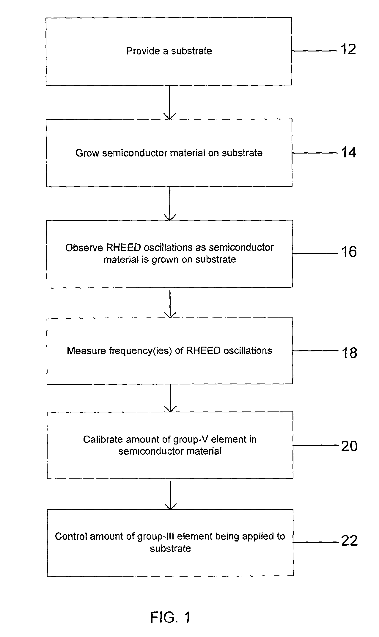
[0031] FIG. 1 is a flowchart describing the process of growing a DBR in one embodiment. Block 12 shows the step of providing a substrate on which DBR materials are grown. Block 14 shows the step of growing semiconductor material on the substrate. As described herein, molecular beam epitaxy is used in this embodiment to grow the materials on the substrate. Block 16 shows the step of observing RHEED oscillations to monitor the composition of group V elements such as antimony (Sb) in the semiconductor material. The RHEED oscillations occur simultaneously as semiconductor material is being grown on the substrate. Growth continues as measurements are taken of the RHEED oscillations.

[0032] The RHEED oscillations are used to monitor the amount of a group V element's atoms being to the substrate. Block 18 shows the next step, in which measurements of the oscillation frequencies are taken and used to control the amounts of the group V elements incorporated into the semiconductor material. Ad...


PUM

PropertyMeasurementUnit
telecommunications-important wavelengthaaaaaaaaaa
temperatureaaaaaaaaaa
band-gap wavelengthaaaaaaaaaa

Abstract

A distributed Bragg reflector (DBR) for a vertical cavity surface emitting laser (VCSEL) includes alternating layers of different semiconductor materials to improve thermal and electrical characteristics for the VCSEL. Use of particular materials reduces the thermal resistivity of the DBR and allows heat to dissipate quickly during operation of the VCSEL.

Description

[0001] The contents of this application are related to those provisional applications having Ser. Nos. 60 / 227,165, 60 / 227,161, and 60 / 226,866, filed Aug. 22, 2000, and a provisional application having Ser. No. 60 / 262,541, filed Jan. 16, 2001. The present application claims priority to these related provisional patent applications and their contents are hereby incorporated by reference in their entirety into the present disclosure. The contents of this application are also related to several nonprovisional patent applications being filed concurrently herewith. These nonprovisional patent applications are hereby incorporated by reference in their entirety and have the following attorney docket reference numerals: 510015-263, 510015-264, 510015-265, 510015-266, 510015-268, 510015-269, 510015-270, 510015-271, and 510015-272.[0003] 1. Field of the Invention[0004] The invention relates in general to a vertical cavity surface emitting laser (VCSEL). More particularly, the invention relates...

Claims


Application Information

Patent Timeline
Patent Type & Authority Applications(United States)
IPC IPC(8): H01S5/024H01S5/042H01S5/183H01S5/30H01S5/323H01S5/343
CPCB82Y20/00H01S5/02461H01S5/18305H01S5/18316H01S5/18344H01S5/305H01S5/3095H01S5/34306
Inventor COLDREN, LARRY A.ALMUNEAU, GUILHEM
Owner RGT UNIV OF CALIFORNIA
Why Eureka
Try Eureka