Stacked package structure of image sensor

a technology of image sensor and package structure, which is applied in the direction of semiconductor/solid-state device manufacturing, electrical apparatus, semiconductor devices, etc., can solve the problems of increasing manufacturing costs, inability to make small products, thin, and slight effects

Inactive Publication Date: 2002-07-25
KINGPAK TECH INC
View PDF0 Cites 167 Cited by
  • Summary
  • Abstract
  • Description
  • Claims
  • Application Information

AI Technical Summary

Problems solved by technology

Therefore, in order to individually package each of the signal processing units and the image sensor, a plurality of substrate and package bodies have to be used, thereby increasing the manufacturing costs.
F...

Method used


Image

  • Stacked package structure of image sensor
  • Stacked package structure of image sensor
  • Stacked package structure of image sensor

Examples


Embodiment Construction

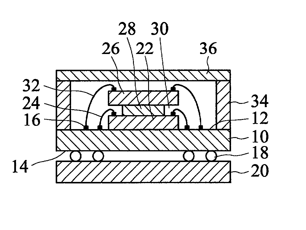
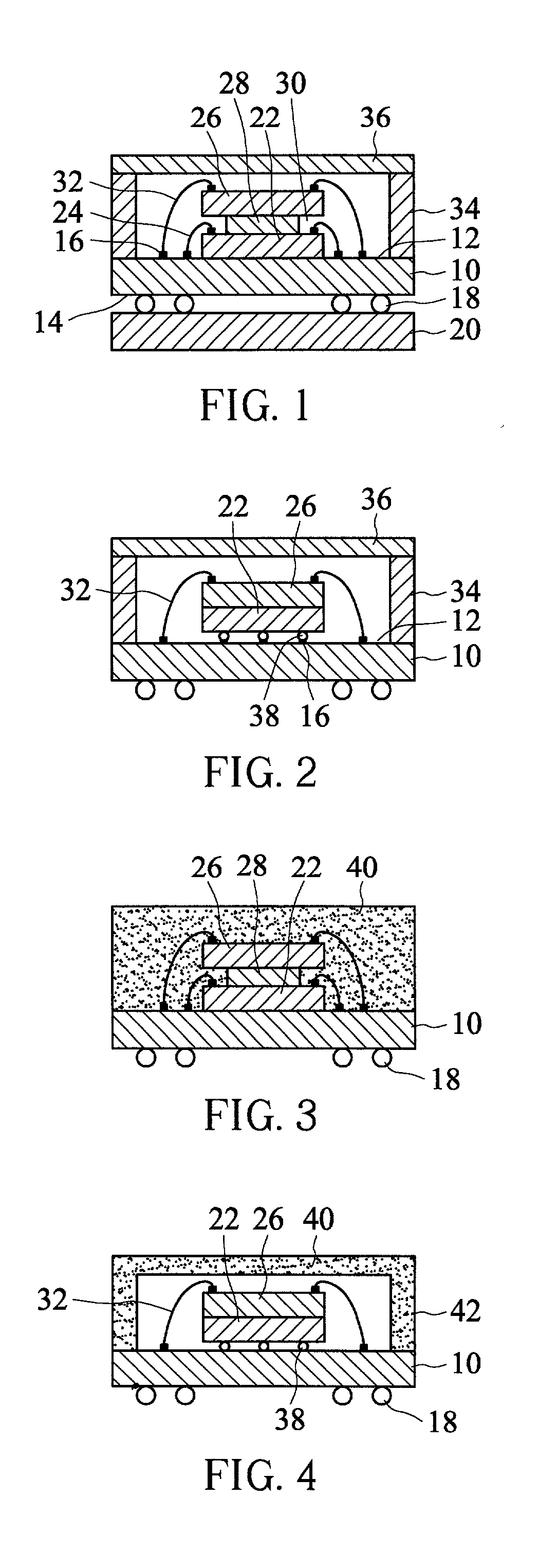
[0018] Referring to FIG. 1, the stacked package structure of the image sensor includes a substrate 10, an integrated circuit 22, an image sensing chip 26, a projection layer 34, and a transparent layer 36.

[0019] The substrate 10 has a first surface 12 and a second surface 14 opposite to the first surface 12. The first surface 12 is formed with signal input terminals 16. The second surface 14 is formed with signal output terminals 18, which may be metallic balls arranged in the form of a ball grid array, for electrically connecting to a printed circuit board 20. Thus, the signals form the substrate 10 can be transmitted to the printed circuit board 20.

[0020] The integrated circuit 22 may be a signal processing unit such as a digital signal processor, a micro processor, a central processing unit (CPU), or the like. The integrated circuit 22 is arranged on the first surface 12 of the substrate 10 and is electrically connected to the signal input terminals 16 of the substrate 10 by way ...


PUM


Abstract

A stacked package structure of an image sensor for electrically connecting to a printed circuit board includes a substrate, an integrated circuit, an image sensing chip, and a transparent layer. The substrate has a first surface and a second surface opposite to the first surface. The first surface is formed with signal input terminals. The second surface is formed with signal output terminals for electrically connecting the substrate to the printed circuit board. The integrated circuit is mounted on the first surface of the substrate and electrically connected to the signal input terminals of the substrate. The image sensing chip is located above the integrated circuit to form a stacked structure with the integrated circuit for electrically connecting to the signal input terminals of the substrate. The transparent layer covers the image sensing chip. The image sensing chip receives image signals via the transparent layer and converts the image signals into electrical signals that are to be transmitted to the substrate. Thus, the image sensing chip of the image sensing product and the integrated circuit can be integrally packaged.

Description

[0001] 1. Field of the Invention[0002] The invention relates to a stacked structure of an image sensor, in particular, to a structure in which integrated circuits and image sensing chips, both having different functions, are packaged into a package body so as to reduce the number of package substrates and to integrally package the integrated circuits and image sensing chips both having different functions.[0003] 2. Description of the Related Art[0004] A general sensor is used for sensing signals, which may be optical or audio signals. The sensor of the invention is used for receiving image signals and transforming the image signals into electrical signals that are transmitted to a printed circuit board.[0005] A general image sensor is used for receiving image signals and converting the image signals into electrical signals that are transmitted to a printed circuit board. The image sensor is then electrically connected to other integrated circuits to have any required functions. For ...

Claims


Application Information

Patent Timeline
IPC IPC(8): H01L31/0203
CPCH01L31/0203H01L2224/16H01L2224/48227H01L2224/48091H01L2924/00014H01L2224/0401
Inventor TU, HSIU WENCHEN, WEN CHUANHO, MON NANCHEN, LI HUANYEH, NAI HUAHUANG, YEN CHENGCHIU, YUNG SHENGLEE, WEN TSANLIU, JOELEE, WU HSIANGTSAI, MENG RU
Owner KINGPAK TECH INC
Why Eureka
Try Eureka