Display apparatus and display control method

a display and control method technology, applied in the field of display apparatuses, can solve the problems of accelerating degradation, lowering the display quality of the display apparatus, and excessive luminance of light emitted from the light-emitting element, so as to reduce the rise of the enhance contrast and image quality, and increase the peak luminance of the display.

Active Publication Date: 2005-03-31
SAMSUNG DISPLAY CO LTD +1
View PDF8 Cites 227 Cited by
  • Summary
  • Abstract
  • Description
  • Claims
  • Application Information

AI Technical Summary

Benefits of technology

[0016] The present invention can increase peak luminance of a display having a high gray scale level (for example, white) while reducing a rise in the luminance of a display having a low gray scale level (for example, black), making it possible to enhance the contrast and the image quality.
[0017] The present invention also can delay degradation of display elements.
[0018] The present invention also can reduce changes in the luminance of light emitted from display elements due to temperature changes.

Problems solved by technology

Another problem with displays using light-emitting elements arises when the light-emitting elements are used for a long period of time.
However, simply decreasing the display luminance of light-emitting elements to delay their degradation lowers the display quality of the display apparatus.
This means that the luminance of light emitted from a light-emitting element may excessively increase due to temperature variation, which may accelerate the degradation.
Conversely, if the luminance of light emitted from the light-emitting element is reduced due to temperature variation, the image quality will be deteriorated.

Method used


Image

  • Display apparatus and display control method
  • Display apparatus and display control method
  • Display apparatus and display control method

Examples


first embodiment

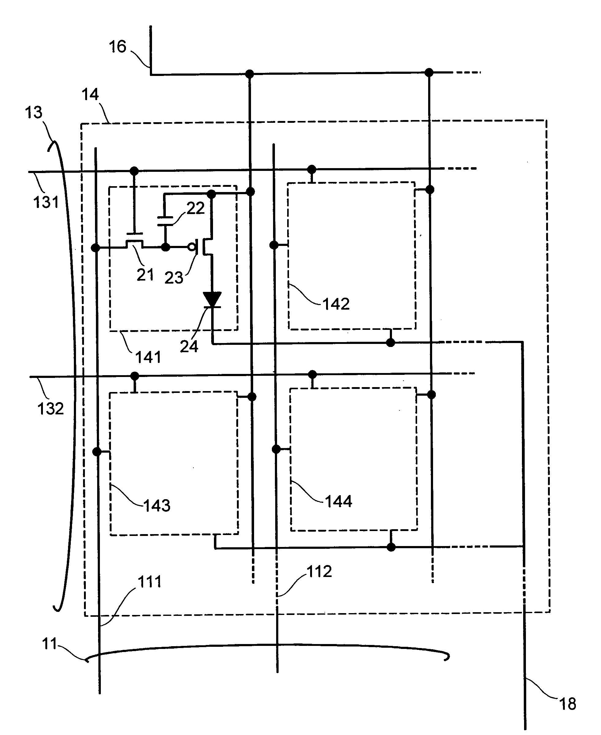
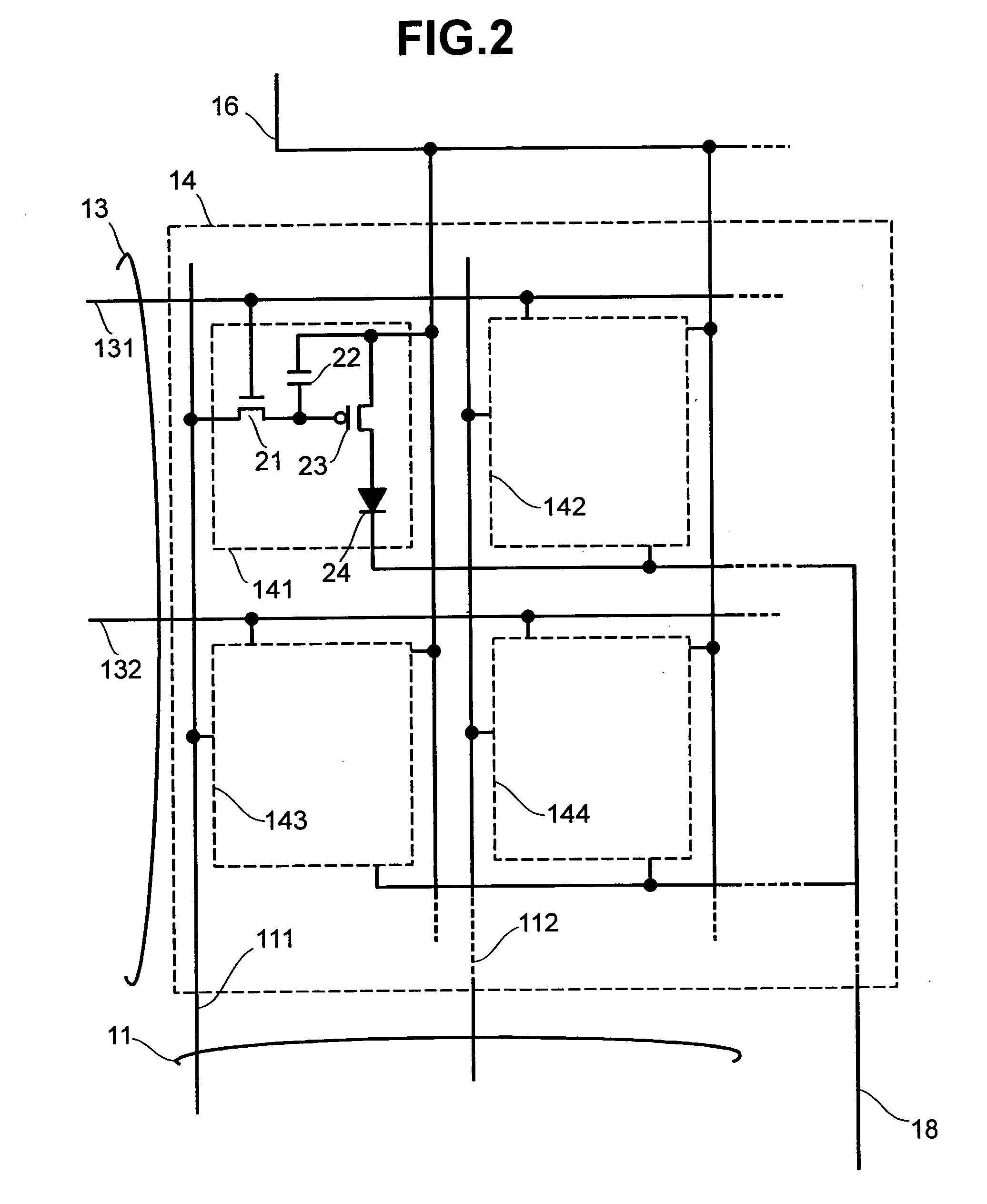
[0044] the present invention will be described below in detail with reference to the accompanying drawings.

[0045] Based on the fact that the luminance of light emitted from a light-emitting element is proportional to the amount of current flowing through the element, the first embodiment of the present invention measures the total amount of current flowing in the light-emitting elements of a display apparatus to obtain average luminance information on its display screen. When the average luminance level is high, the voltage applied to the light-emitting elements is controlled so as to reduce the actual display luminance level of each element. Measuring the total amount of current flowing in the light-emitting elements of the display apparatus also makes it possible to reduce changes in the average luminance level of the display apparatus and in the luminance of light emitted from the light-emitting elements due to temperature changes.

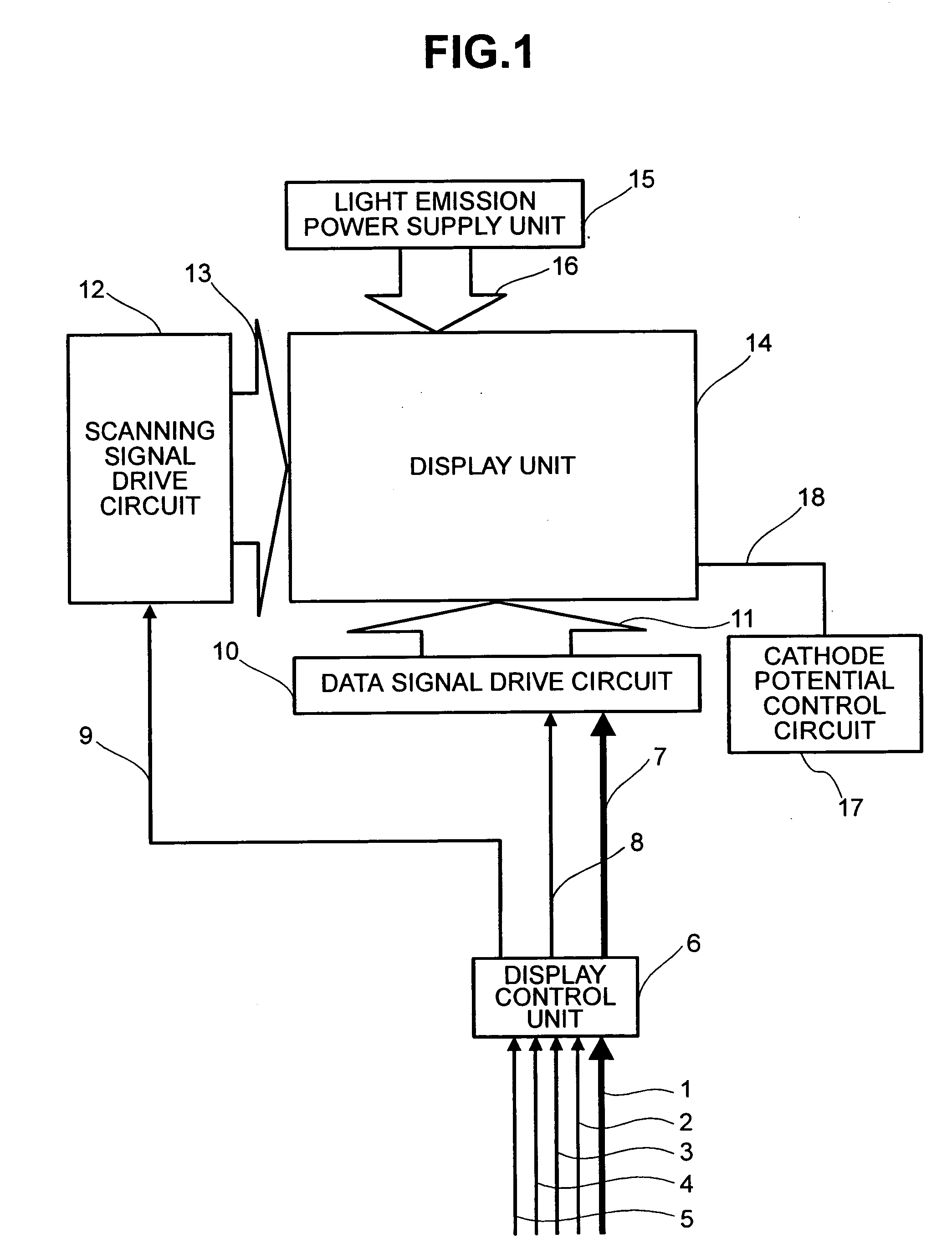
[0046]FIG. 1 shows a light-emitting element disp...

second embodiment

[0064] the present invention will be described in detail with reference to accompanying drawings.

[0065] The second embodiment of the present invention controls the output signal voltage of a signal line driving means according to average luminance information to control the display luminance of the screen.

[0066]FIG. 10 shows a configuration example of an organic EL element display apparatus according to the second embodiment of the present invention. Most of the components are the same as those used by the first embodiment of the present invention shown in FIG. 1. Each component in FIG. 10 operates in the same way as the corresponding component in FIG. 1. However, the second embodiment newly employs a data signal drive circuit with output control capability 19, instead of the data signal drive circuit 10 of the first embodiment. The data signal drive circuit with output control capability 19 converts the analog display data signal 7 according to the average luminance information 17...

third embodiment

[0069] the present invention will be described in detail with reference to accompanying drawings.

[0070] The third embodiment of the present invention controls the display luminance of the screen by performing digital signal processing on the display data signal entered from outside according to average luminance information and thereby converting the display data.

[0071]FIG. 12 shows a configuration example of an organic EL element display apparatus according to the third embodiment of the present invention. Most of the components are the same as those used by the first embodiment of the present invention shown in FIG. 1. Each component in FIG. 12 operates in the same way as the corresponding component in FIG. 1. However, the third embodiment newly employs a signal conversion unit 60, instead of the display control unit 6. The signal conversion unit 60 has the following functions in addition to those of the display control unit 6.

[0072]FIG. 13 shows how the signal conversion unit 6...


PUM


Abstract

The present invention comprises: a display unit having a plurality of pixels arranged therein, each pixel including an organic EL element 24, a switching TFT, and a drive TFT; a data signal drive circuit for receiving image data for each frame period and outputting an image signal based on the image data; a scanning signal drive circuit for outputting a scanning signal for controlling a timing at which the switching element of each of the plurality of pixels receives the image signal; and a current source (a light emission power supply unit and a cathode potential control circuit together) for outputting a current supplied to the light emitting unit of each of the plurality of pixels through its drive element; wherein the current source modulates the value of the output current within each frame period.

Description

BACKGROUND OF THE INVENTION [0001] The present invention relates to a display apparatus employing EL (Electro Luminescence) elements, organic EL elements, or other light-emitting type display elements (light-emitting elements), and a drive method therefor. [0002] Light-emitting (or self-luminous) elements have the characteristic that the luminance of light emitted from them is proportional to the amount of current flowing through them, making it possible to provide a gray scale display by controlling the amount of current flowing in the elements. A plurality of such light-emitting elements may be arranged so as to form a display apparatus. [0003] Displays using active matrix light-emitting elements are advantageous over those using simple matrix light-emitting elements in the luminance of the screen and power consumption. Each pixel of a display using active matrix light-emitting elements, however, requires a TFT (Thin Film Transistor) element capable of performing accurate V-I conv...

Claims


Application Information

Patent Timeline
Patent Type & Authority Applications(United States)
IPC IPC(8): G09G3/20G09G3/32
CPCG09G3/2014G09G3/3208G09G3/3233G09G2320/066G09G2320/029G09G2320/041G09G2320/043G09G2320/0238
Inventor AWAKURA, HIROKIKASAI, NARUHIKOFURUHASHI, TSUTOMUSATOU, TOSHIHIRO
Owner SAMSUNG DISPLAY CO LTD
Why Eureka
Try Eureka