Method of manufacturing polarizing plate, method of manufacturing display apparatus having the same and the display apparatus

a technology of polarizing plate and manufacturing method, which is applied in the direction of polarizing elements, instruments, other domestic objects, etc., can solve the problems of reducing the luminance of the liquid crystal display apparatus, low thermal resistance reducing the light use efficiency of the conventional polarizing plate, so as to improve the characteristics of the polarizing plate, improve the efficiency of the manufacturing process, and improve the luminance of the display apparatus

Active Publication Date: 2013-04-11
SAMSUNG DISPLAY CO LTD
View PDF3 Cites 3 Cited by
  • Summary
  • Abstract
  • Description
  • Claims
  • Application Information

AI Technical Summary

Benefits of technology

[0029]According to the embodiments of the present invention, the polarizing plate includes a metal layer so that light having a direction different from a direction of a polarizing axis can be reflected to the backlight assembly and reused. As a consequence, a luminance of the display apparatus can be improved.
[0030]A metal ink is transferred on the protruding portions of the resist pattern to form the metal layer so that an etching process can be omitted. As a consequence, a manufacturing process can be simplified, characteristics of the polarizing plate can be improved, and a manufacturing cost can be decreased.

Problems solved by technology

The conventional polarizing plate has low thermal resistance.
The conventional polarizing plate may absorb about half of light emitted from the backlight assembly, so light use efficiency is decreased, thus decreasing a luminance of the liquid crystal display apparatus.
However, wire grid polarizing plates including the metal pattern in which each metal portion has a small width and a small gap are difficult to manufacture.
A shape of the metal pattern is difficult to control in an etching process and a manufacturing cost increases.

Method used


Image

  • Method of manufacturing polarizing plate, method of manufacturing display apparatus having the same and the display apparatus
  • Method of manufacturing polarizing plate, method of manufacturing display apparatus having the same and the display apparatus
  • Method of manufacturing polarizing plate, method of manufacturing display apparatus having the same and the display apparatus

Examples


Embodiment Construction

[0041]Hereinafter, the embodiments of the present invention will be described in detail with reference to the accompanying drawings.

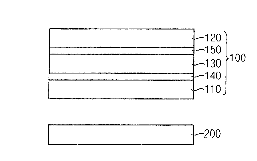
[0042]FIG. 1 is a cross-sectional view illustrating a display apparatus according to an exemplary embodiment of the present invention.

[0043]Referring to FIG. 1, the display apparatus includes a display panel 100 and a backlight assembly 200.

[0044]The display panel 100 includes a first display substrate 110, a second display substrate 120, a liquid crystal layer 130, a first polarizing plate 140 and a second polarizing plate 150.

[0045]The first display substrate 110 includes pixel electrodes. The first display substrate 110 further includes a plurality of gate lines extending in a first direction, a plurality of data lines extending in a second direction crossing the first direction and a plurality of switching elements connected to the gate lines and the data lines.

[0046]The second display substrate 120 faces the first display substrate 110. The second ...


PUM

PropertyMeasurementUnit
widthaaaaaaaaaa
widthaaaaaaaaaa
diameteraaaaaaaaaa

Abstract

A method of manufacturing a polarizing plate includes disposing a non-conductive material on a base substrate, pressing the non-conductive material using a mold and forming a resist pattern, the resist pattern including a plurality of protruding portions, and forming a metal layer on the protruding portions of the resist pattern. Accordingly, a luminance of a display apparatus can be improved and a manufacturing process can be simplified.

Description

CROSS-REFERENCE TO RELATED APPLICATION[0001]This application claims priority to Korean Patent Application No. 10-2011-103691 filed on Oct. 11, 2011, the contents of which are incorporated by reference herein in their entireties.TECHNICAL FIELD[0002]Exemplary embodiments of the present invention relate to a method of manufacturing a polarizing plate, a method of manufacturing a display apparatus having the polarizing plate, and a display apparatus. More particularly, exemplary embodiments of the present invention relate to a method of manufacturing a polarizing plate, which can improve a luminance of a display apparatus and simplify a manufacturing process, and a method of manufacturing a display apparatus having the polarizing plate, and a display apparatus.DISCUSSION OF THE RELATED ART[0003]Generally, liquid crystal display apparatuses have a thin thickness, a light weight, and low power consumption and are used for monitors, laptop computers, cellular phones, televisions and so on...

Claims


Application Information

Patent Timeline
Patent Type & Authority Applications(United States)
IPC IPC(8): G02F1/1335B05D5/12B05D5/06
CPCG02F1/133528G02B5/3058G02F2001/133548G02F1/133548B29C59/02B29D7/01G02B5/30G02F1/1335
Inventor JANG, DAE-HWANTAKAKUWA, ATSUSHI
Owner SAMSUNG DISPLAY CO LTD
Why Eureka
Try Eureka