

Schottky gate field effect transistor
a field effect transistor and gate field technology, applied in the direction of basic electric elements, electrical equipment, semiconductor devices, etc., can solve the problems of degrading distortion characteristics during operation and inconvenien
- Summary
- Abstract
- Description
- Claims
- Application Information
AI Technical Summary
Problems solved by technology
Method used
Image

Examples
first embodiment
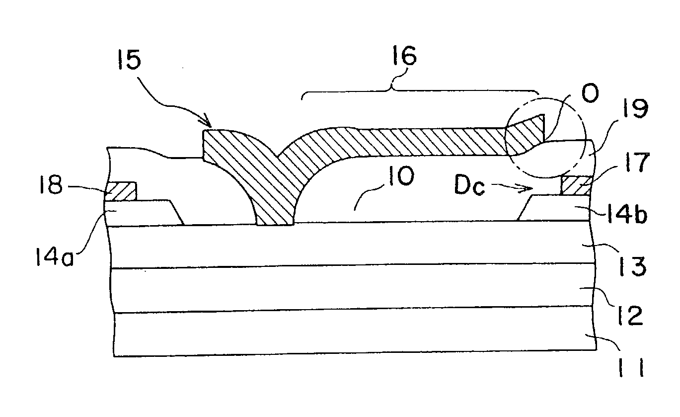
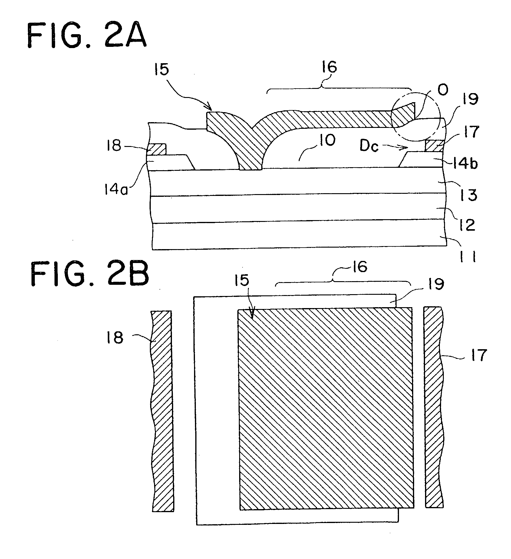
[0027] As shown in FIGS. 2A and 2B, a Schottky gate FET includes a buffer layer 12, a channel layer 13, a source contact layer 14a and a drain contact layer 14b sequentially overlying a semi-insulating GaAs substrate 11. A gate electrode 15 in Schottky contact with the channel layer 13, and a source electrode 18 and a drain electrode 17 are formed in and over the recess 10 formed by removing part of the contact layers 14a and 14b.
[0028] The gate electrode 15 includes a T-shaped gate extension (field plate) 16 extending toward the drain electrode 17. The gate extension 16 is positioned such that the gate extension 16 is vertically overlapped with part of a drain contact region "Dc" including the drain contact layer 14b and the drain electrode 17. The end of the gate extension 16 near to the drain contact region "Dc" is separated from both of the drain electrode 17 and the drain contact layer 14b by 2.5 .mu.m or more, and preferably by 3.0 .mu.m or more. None of drain electrode 17 and...
second embodiment
[0041] As shown in FIGS. 5A and 5B, in the Schottky gate FET of the present embodiment, the central section of the gate extension 16 of the first embodiment is removed so that a field plate 16A is independently mounted on the dielectric film 19. To the field plate 16A is applied a potential similar to the potential applied to the gate electrode 15 through interconnect not shown in the drawings. Similarly to the first embodiment, the end of the separated field plate 16A of the second embodiment near to the drain contact region "Dc" is also separated from both of the drain electrode 17 and the drain contact layer 14b by 2.5 .mu.m or more, and preferably by 3.0 .mu.m or more.
[0042] Since the Schottky gate FET of the present embodiment has the field plate 16A separated from the gate electrode 15, the effect of reducing the parasitic capacitance between the field plate 16A and the channel layer 13 can be obtained in addition to the effects of the first embodiment. The Schottky gate FET o...
third embodiment
[0043] As shown in FIGS. 6A and 6B and similarly to the second embodiment, in the Schottky gate FET of the present embodiment, the separated field plate 16A is separated from the gate electrode 15. However, the thickness of the dielectric film 19 immediately below the field plate 16A is thinner than that shown in FIG. 5A, or the thickness is 50 to 200 nm, for example. Therefore, in addition to the effects of the second embodiment, the effect of suppressing the phenomenon of reducing the current after the operation at the excessive power is further increased so that the current reduction can be prevented even if the further excessive power is input.
[0044] Further, in the present embodiment, the drain electrode 17 and the drain contact layer 14b can be formed by moving the positions thereof to the right-hand direction in FIG. 6A. Also, in this case, the end of the field plate 16A near to the drain contact region "Dc" can be separated from both of the drain electrode 17 and the drain c...
PUM
 Abstract
Description
Claims
Application Information