Electrostatic discharge protection device and network with high voltage tolerance

a protection device and high voltage technology, applied in the direction of emergency protective arrangements for limiting excess voltage/current, electrical apparatus, transistors, etc., can solve the problems of permanent damage to the mos device and the inability of the pad to tolerate higher than vdd 3

Inactive Publication Date: 2004-12-23
HU DAVID YU
View PDF5 Cites 35 Cited by
  • Summary
  • Abstract
  • Description
  • Claims
  • Application Information

AI Technical Summary

Problems solved by technology

The rapid charge transfer generates voltages large enough to breakdown insulating films, such as gate oxide, and to cause permanent damage to the MOS device.
However, such PMOS with its bulk tied to ...

Method used


Image

  • Electrostatic discharge protection device and network with high voltage tolerance
  • Electrostatic discharge protection device and network with high voltage tolerance
  • Electrostatic discharge protection device and network with high voltage tolerance

Examples


Embodiment Construction

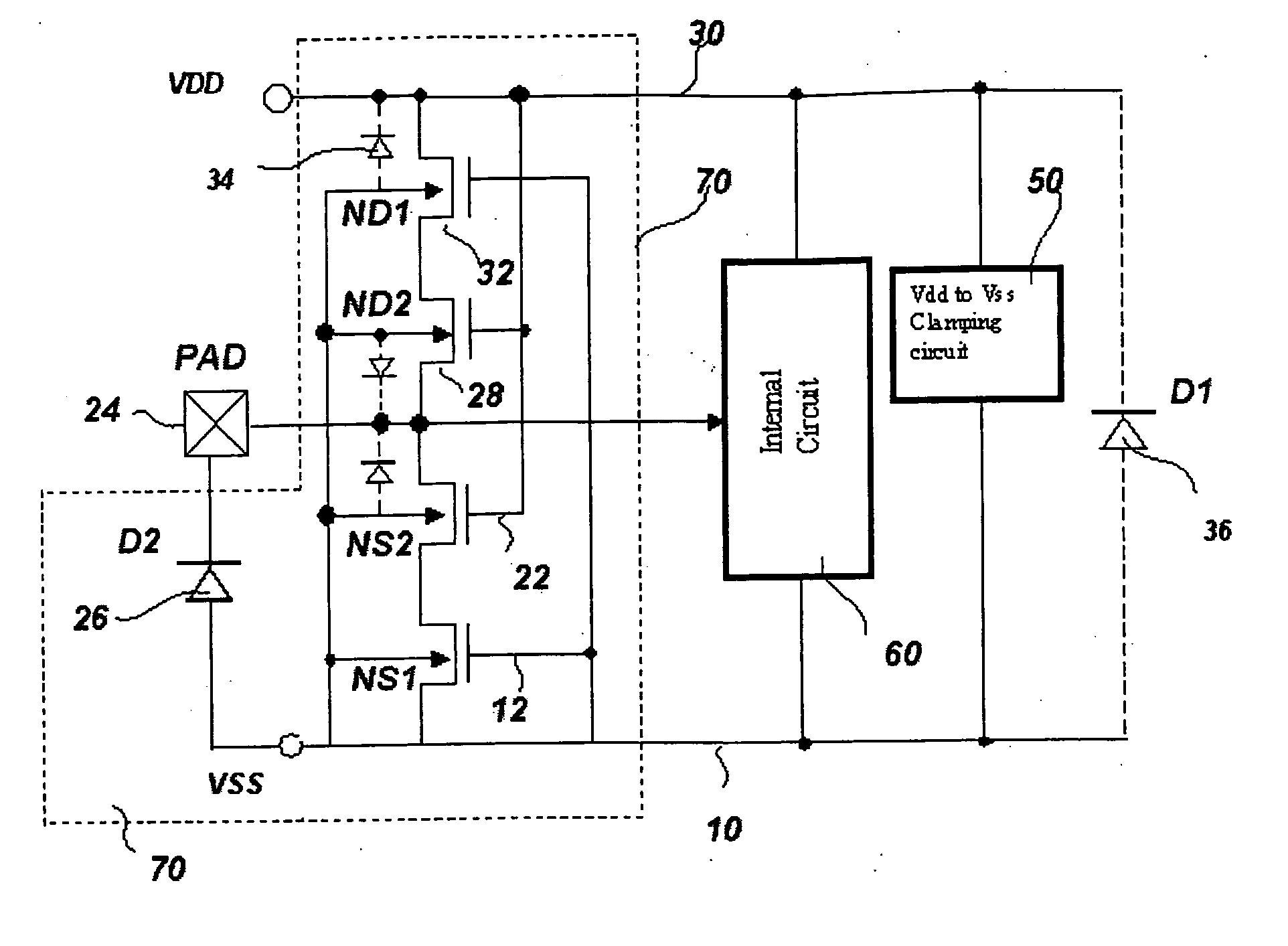
[0039] Refer now to the FIG. 4. In between the PAD 24 and VDD 30 there are two cascaded VDD_NMOS. The first VDD_NMOS (ND1) 32 which source diffusion is connected to VDD 30 and its drain shares the same diffusion with the second VDD_NMOS (ND2) 28. The drain of the second VDD_NMOS 28 is connected directly to the PAD 24.

[0040] Of the similar fashion, two cascaded VSS_NMOS are found in between the PAD 24 and the ground VSS 10. The gate of first VDD_NMOS 32 and the first VSS_NMOS 12 are tied together and connected to the VSS 10 to ensure the path between the PAD 24 to VDD 30 and VSS 10 are turned off during the normal operation. The gate of the second VDD_NMOS 28 and the gate of the second VSS_NMOS 22 are tied together and connected directly to the VDD 30. The junction diode 26 between the PAD and VSS is inserted to form the protection network 70 at the PAD node.

[0041] Now further refer to the FIG. 5, the cross-sectional view of the Cascaded VDD_NMOS of the first preferred embodiment. Du...


PUM


Abstract

This invention relates to a protection network for electrostatic discharge in between the VDD power line and IO pad or two different power line of two different potentials. In more particular a series devices in combination with at least one NMOS which substrate is completely isolated from its N-diffusion to form a protection network between the IO pad and Vdd line so that the IO pad can sustain high voltage than the VDD power. Different embodiments are shown. The application of such device or devices is independent of voltage difference and the power on or off sequence. Further more those devices can be used when hot-plug is required which means inserting such device during the power on would not introduce any significant transient leakage current between the IO pad and Vdd.

Description

[0001] (1) Field of the Invention[0002] The present invention relates in general to a semiconductor device and circuit for electrostatic discharge (ESD) protection. In more particular, to the protection clamp therefore made by such devices between the power line and the I / O pad whereby the IO pad node is able to sustain higher voltage than the power line during the normal operation.[0003] (2) Description of the Prior Art[0004] Electrostatic discharge is an event where sudden charges transfer between one body to another. The rapid charge transfer generates voltages large enough to breakdown insulating films, such as gate oxide, and to cause permanent damage to the MOS device. Normal way of ESD protection is to build integrated circuits of various structures on the input and output pins to shunt ESD currents away from sensitive internal structures.[0005] FIG. 1 (Prior Art) shows a typical ESD protection network. In this circuit, an internal circuit voltage, SIGNAL 20, is propagated to...

Claims


Application Information

Patent Timeline
IPC IPC(8): H01L27/02H02H9/00
CPCH01L27/0266
Inventor HU, DAVID YU
Owner HU DAVID YU
Why Eureka
Try Eureka