Magnetic memory device

Active Publication Date: 2005-01-06
SAMSUNG ELECTRONICS CO LTD
View PDF11 Cites 14 Cited by
  • Summary
  • Abstract
  • Description
  • Claims
  • Application Information

AI Technical Summary

Problems solved by technology

In some instances, MRAM devices may experience stray or external magnetic fields that emanate from sources other than the word line and bit lines.

Method used


Image

  • Magnetic memory device
  • Magnetic memory device
  • Magnetic memory device

Examples


Embodiment Construction

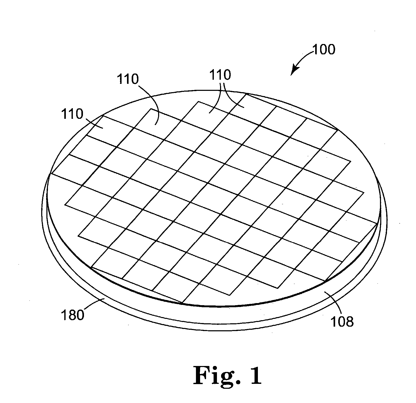
[0025] A perspective view of an exemplary embodiment according to the invention of a simplified magnetic random access memory (MRAM) wafer 100 is presented in FIG. 1. In FIG. 1 and all that follow, it is to be understood that for clarity the various components of the illustrated devices are not necessarily shown to scale. MRAM wafer 100 includes a silicon wafer 108 on one side of which is disposed separable memory chips 110. Each of the separable memory chips 110 includes multiple memory arrays having multiple memory cells (not shown).

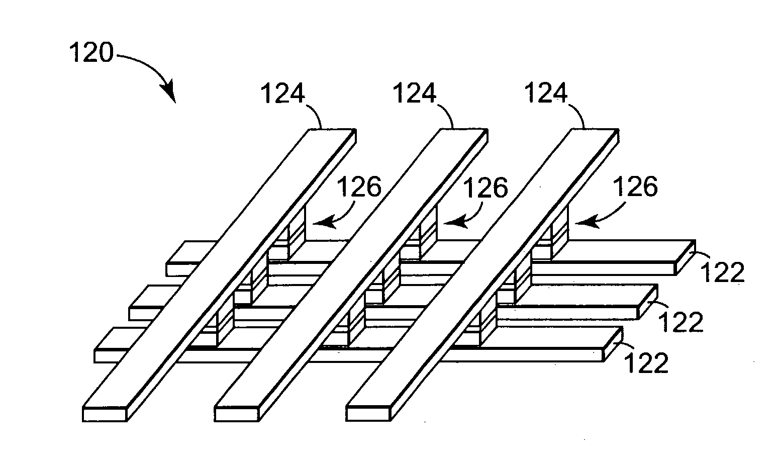
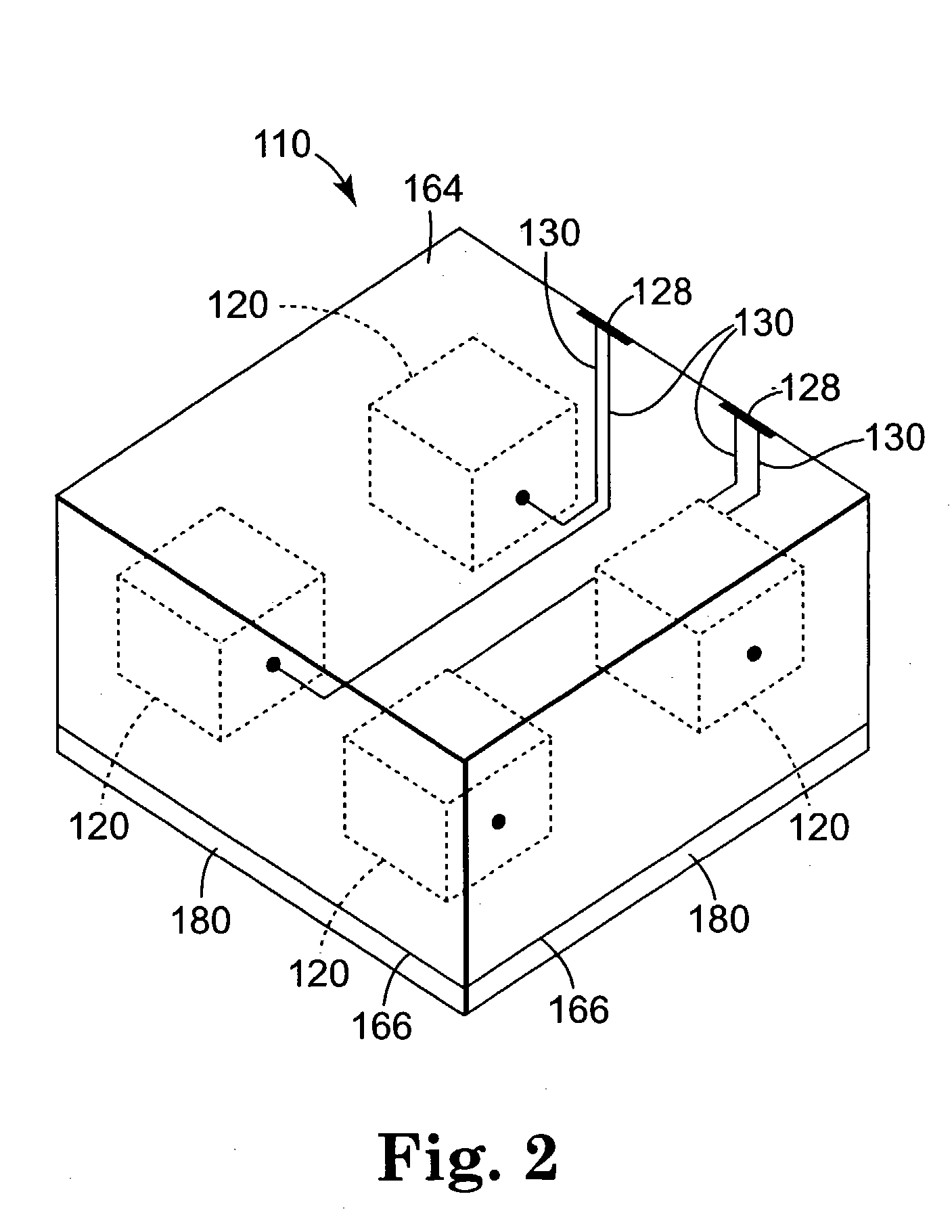
[0026]FIG. 2 illustrates an exemplary embodiment according to the invention of a simplified magnetic memory chip 110 after separation from memory wafer 100. Memory chip 110 has at least one and preferably a plurality of magnetic memory arrays 120. Memory chip 110 includes an exterior chip face 164, at least one bond pad 128, and a second chip surface 166. In the exemplary embodiment illustrated in FIG. 2, a magnetically permeable shield layer 180 exte...


PUM

PropertyMeasurementUnit
Temperatureaaaaaaaaaa
Magnetic fieldaaaaaaaaaa
Permeabilityaaaaaaaaaa

Abstract

A memory device includes a first surface having memory chips disposed thereon, the memory chips defining an exterior face of the memory device, and a second surface opposite the exterior face. A magnetically permeable shield layer extends over at least one of the exterior face and the second surface of the memory device.

Description

THE FIELD OF THE INVENTION [0001] The present invention generally relates to memory devices, and more particularly, to magnetic random access memory (MRAM) devices. BACKGROUND OF THE INVENTION [0002] A magnetic random access memory (MRAM) wafer is generally a silicon wafer onto which is built, or disposed, a group of magnetic memory chips (also know as dies). A typical MRAM wafer might comprise thousands of magnetic memory chips. The magnetic memory chips are sectioned across the MRAM wafer in a grid pattern prior to separation from the MRAM wafer for subsequent use in electronic devices. [0003] The silicon wafer provides a platform on which magnetic memory chips are built. Each magnetic memory chip comprises a plurality of magnetic memory arrays, and each magnetic memory array includes multiple magnetic memory cells. Magnetic memory arrays have intersecting word lines and bit lines. Magnetic memory cells, or memory cells, are formed at the intersection of word lines and bit lines. ...

Claims


Application Information

Patent Timeline
IPC IPC(8): G11C11/15H01L27/10H01L21/8246H01L27/105H01L27/22
CPCG11C11/15H01L27/222H01L2224/48091H01L2224/48247H01L2924/10253H01L2924/3025Y10T428/32Y10T428/325H01L2924/01078H01L2924/00014H01L2924/00H10B61/00
Inventor ANTHONY, THOMAS C.STOBBS, COLIN A.BHATTAHARYYA, MANOJ K.HOLDEN, ANTHONY P.BLOOMQUIST, DARREL R.BLOOMQUIST, JUDY
Owner SAMSUNG ELECTRONICS CO LTD
Why Eureka
Try Eureka