

Pattern formation method and pattern formation apparatus, method for manufacturing device, electro-optical device, electronic device, and method for manufacturing active matrix substrate
a pattern formation apparatus and pattern formation technology, applied in the direction of conductive pattern formation, identification means, instruments, etc., can solve the problems of increasing the cost of such banks as described above, not being able to achieve sufficient accuracy with regard to line width, and liquid drops that are not sufficiently wet and spread ou
- Summary
- Abstract
- Description
- Claims
- Application Information
AI Technical Summary
Benefits of technology
Problems solved by technology
Method used
Image

Examples
second preferred embodiment
[0122] Pattern Formation Method
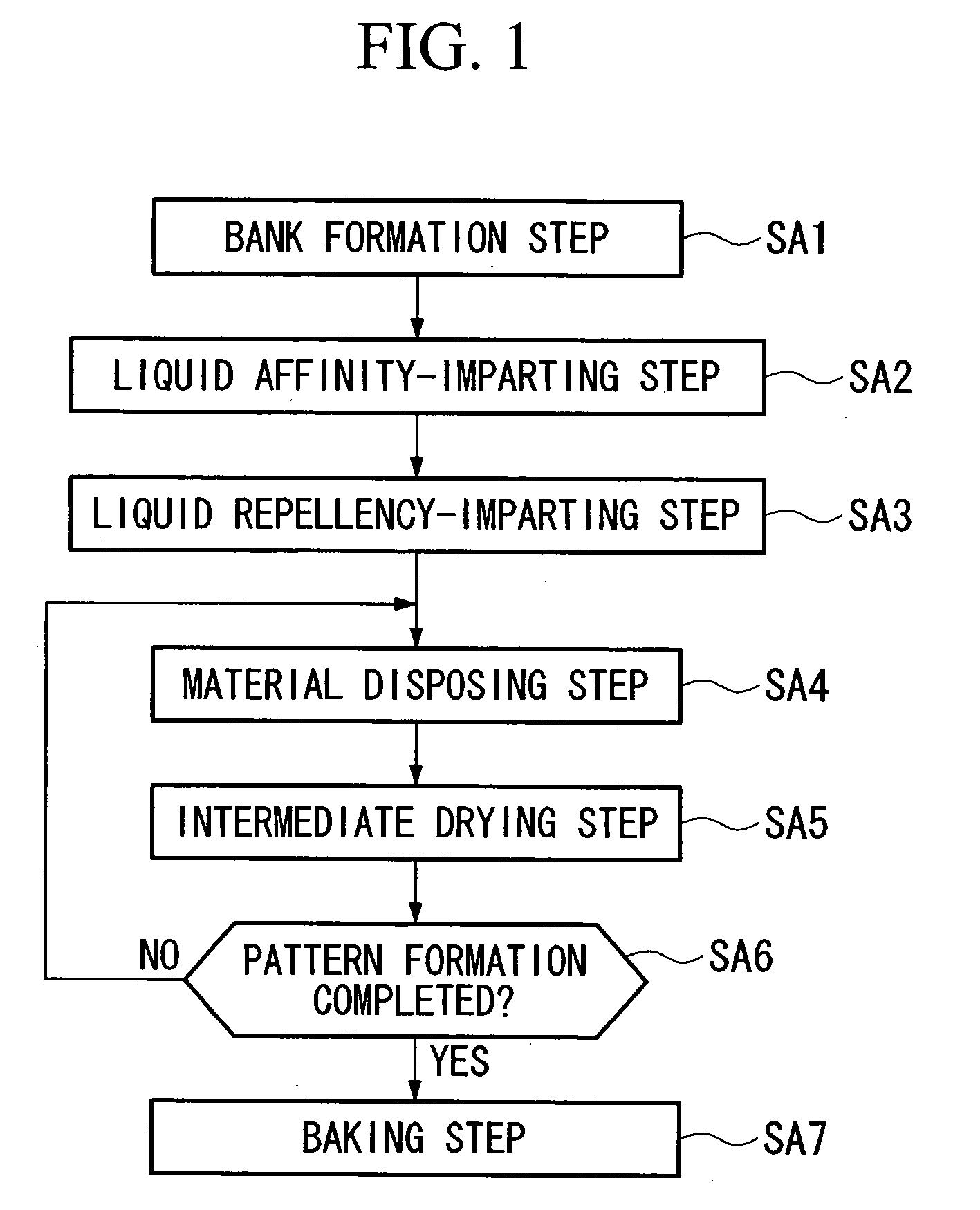
[0123] In the following, a preferred embodiment of the pattern formation method according to the present invention will be explained with reference to the figures. FIG. 9 is a flow chart showing this preferred embodiment of the pattern formation method according to the present invention.
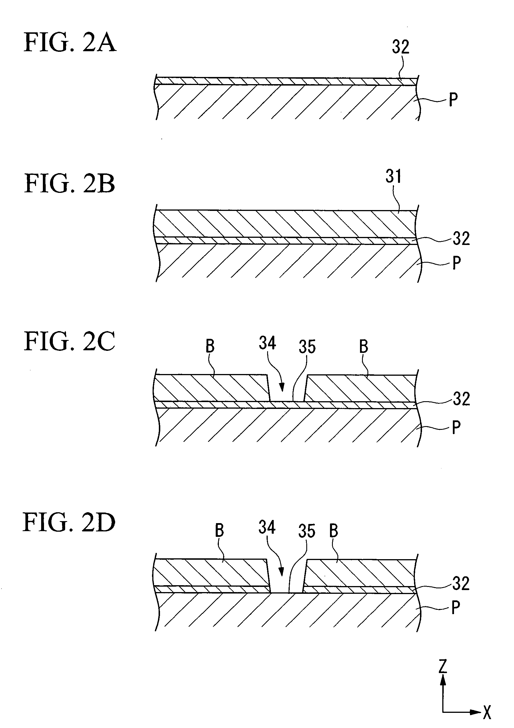
[0124] Here, for this second preferred embodiment of the present invention, an example will be explained in which an electrically conductive film wiring pattern is formed upon a glass substrate. Furthermore, as the functional liquid for making this electrically conductive film wiring pattern, there is used an organic silver compound dissolved in diethylene glycol diethyl ether solvent (a dispersion medium).
[0125] Referring to FIG. 9, the pattern formation method according to this second preferred embodiment of the present invention includes: a substrate cleaning step in which the substrate upon which the liquid drops of a functional liquid are to be disposed is clean...
PUM
| Property | Measurement | Unit |
|---|---|---|
| liquid repellency | aaaaa | aaaaa |
| affinity | aaaaa | aaaaa |
| electrically conductive | aaaaa | aaaaa |
Abstract
Description
Claims
Application Information