Image sensor having an improved transparent layer

a technology of image sensor and transparent layer, which is applied in the direction of electrical equipment, semiconductor devices, radio frequency control devices, etc., can solve the problems of increasing manufacturing costs and complicated manufacturing processes, and achieve the effects of simplifying manufacturing processes, reducing collisions, and increasing the cleanness of transparent layers

Active Publication Date: 2005-01-20
TONG HSING ELECTRONICS IND LTD
View PDF0 Cites 4 Cited by
  • Summary
  • Abstract
  • Description
  • Claims
  • Application Information

AI Technical Summary

Benefits of technology

[0012] Therefore, the transparent layer may be decreased collision and may be increased the cleanness of the transparent layer, therefore, simplifying the manufacturing processes and decreasing the manufacturing cost.

Problems solved by technology

Therefore, the transparent layer 22 have to be wiped and inspected again before the encapsulation thereof, thereby complicating the manufacturing processes and increasing the manufacturing cost.

Method used


Image

  • Image sensor having an improved transparent layer
  • Image sensor having an improved transparent layer
  • Image sensor having an improved transparent layer

Examples


Embodiment Construction

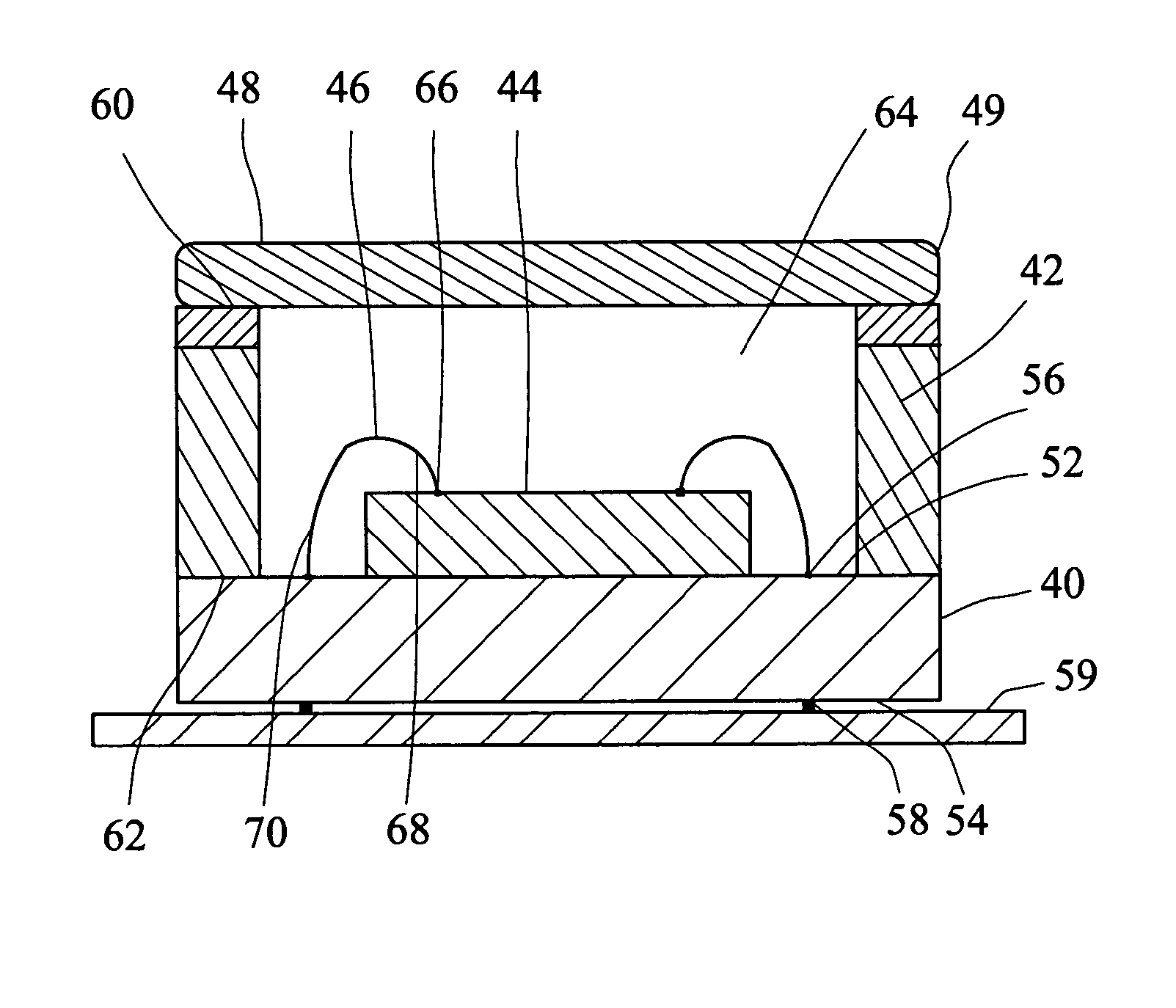
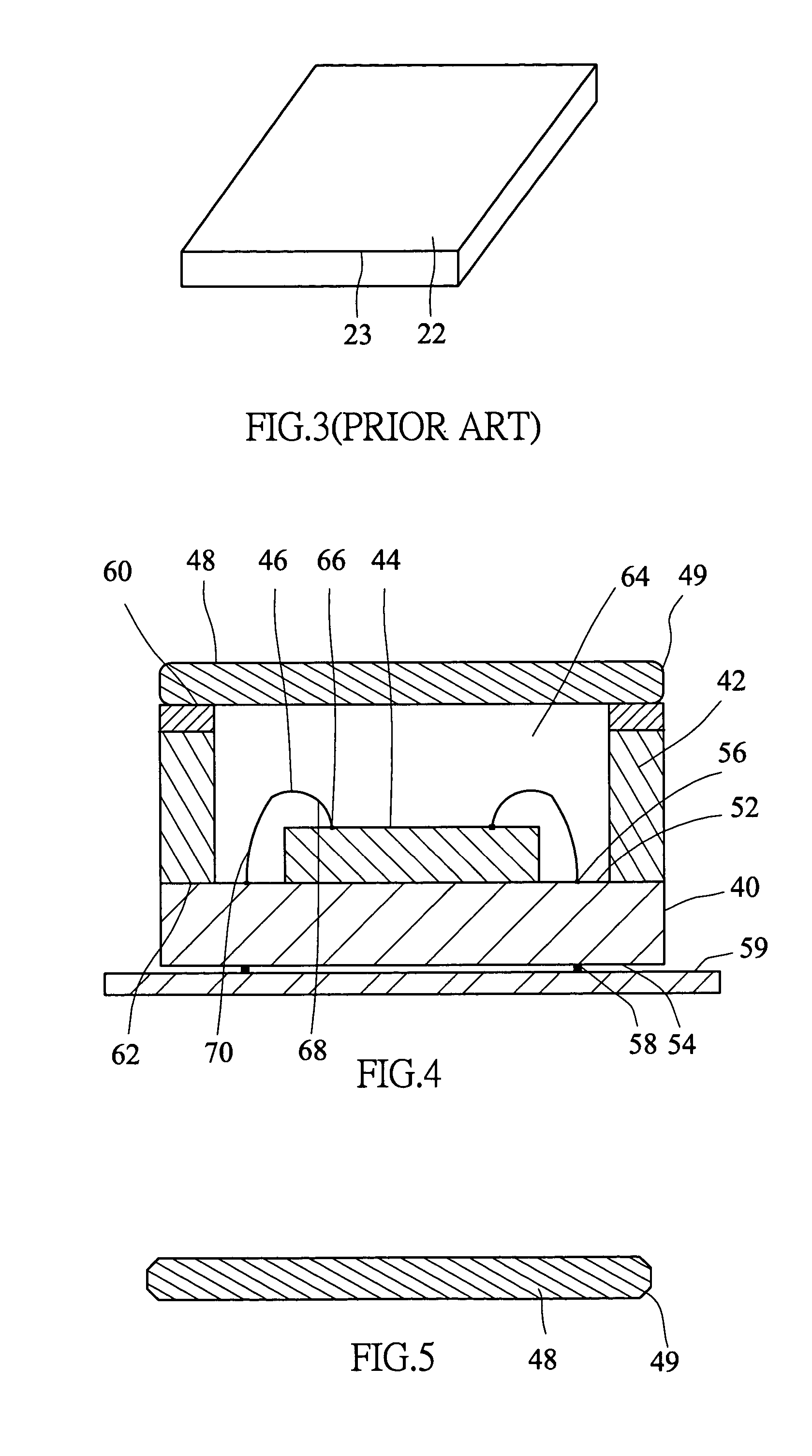
[0018] Please referring to FIG. 4, an image sensor of the present invention includes a substrate 40, a frame layer 42, a photosensitive chip 44, a plurality of wires 46 and a transparent layer 48.

[0019] The substrate 40 has an upper surface 52 and a lower surface 54. The upper surface 52 is formed with a plurality of first terminals 56 projecting over the upper surface 52, and the lower surface 54 is formed with a plurality of second terminals 58 for electrically connecting to a printed circuit board 59.

[0020] The frame layer 42 has a first surface 60 and a second surface 62, the second surface 62 of the frame layer 42 is adhered on the upper surface 52 of the substrate 40 so as to form a cavity 64 together with the substrate 40.

[0021] The photosensitive chip 44 is formed with a plurality of bonding pads 66, and is mounted on the upper surface 52 of the substrate 40 and within the cavity 64.

[0022] The plurality of wires 46, each of which has a first terminal 68 and a second term...


PUM


Abstract

An image sensor having an improved transparent layer includes a substrate, a frame layer, a photosensitive chip, a plurality of wires, and a transparent layer. The substrate has an upper surface formed with a plurality of first connected points. The frame layer is arranged on the upper surface of the substrate so as to form a cavity together with the substrate. The photosensitive chip is mounted on the upper surface of the substrate and within the cavity. The plurality of wires are electrically connected the photosensitive chip to the first connected point of the substrate. The transparent layer is covered on the frame layer for covering the photosensitive chip so that the photosensitive chip may receive optical signals passing through the transparent layer, respectively, at the peripheries of the transparent layer are formed with cut-corners. Therefore, the transparent layer may be decreased collision and may be increased the cleanness of the transparent layer, therefore, simplifying the manufacturing processes and decreasing the manufacturing cost.

Description

BACKGROUND OF THE INVENTION [0001] 1. Field of the Invention [0002] The invention relates to an image sensor having an improved transparent layer, and in particular to an image sensor that has an improved transparent layer, and may be manufactured more conveniently. [0003] 2. Description of the Related Art [0004] A general sensor is used to sense signals, which may be optical or audio signals. The sensor of the invention is used to receive image signals or optical signals. After receiving the image signals, the sensor converts the image signals into electrical signals, which are then transmitted to a printed circuit board via a substrate. [0005] Referring to FIG. 1, a conventional image sensor includes a substrate 10, a frame layer 12, a photosensitive chip 14, a plurality of wires 15, and a transparent layer 22. The substrate 10 has an upper surface 11 on which first terminals 18 are formed, and a lower surface 13 on which second terminals 24 are formed. The frame layer 12 is adher...

Claims


Application Information

Patent Timeline
Patent Type & Authority Applications(United States)
IPC IPC(8): H01L31/0203H01L31/0232
CPCH01L31/0203H01L2224/48091H01L2224/48227H01L2924/00014
Inventor HSIEH, JACKSONWU, JICHENWEL, CHANNINGLIN, BIRD
Owner TONG HSING ELECTRONICS IND LTD
Why Eureka
Try Eureka