Isolation structure for deflectable nanotube elements

Active Publication Date: 2005-02-17
NANTERO
View PDF54 Cites 97 Cited by
  • Summary
  • Abstract
  • Description
  • Claims
  • Application Information

AI Technical Summary

Problems solved by technology

However, the density of bipolar digital integrated circuits is limited by their high power consumption and the ability of packaging technology to dissipate the heat produced while the circuits are operating.
The density and operating speed of MOS digital circuits are still limited by the need to dissipate the heat produced when the device is operating.
Digital logic integrated circuits constructed from bipolar or MOS devices do not function correctly under conditions of high heat or extreme environments.
As leakage current increases, the operating temperature of the device rises, the power consumed by the circuit increases, and the difficulty of discriminating the off state from the on state reduces circuit reliability.
Conventional digital logic circuits also short inter

Method used


Image

  • Isolation structure for deflectable nanotube elements
  • Isolation structure for deflectable nanotube elements
  • Isolation structure for deflectable nanotube elements

Examples


Embodiment Construction

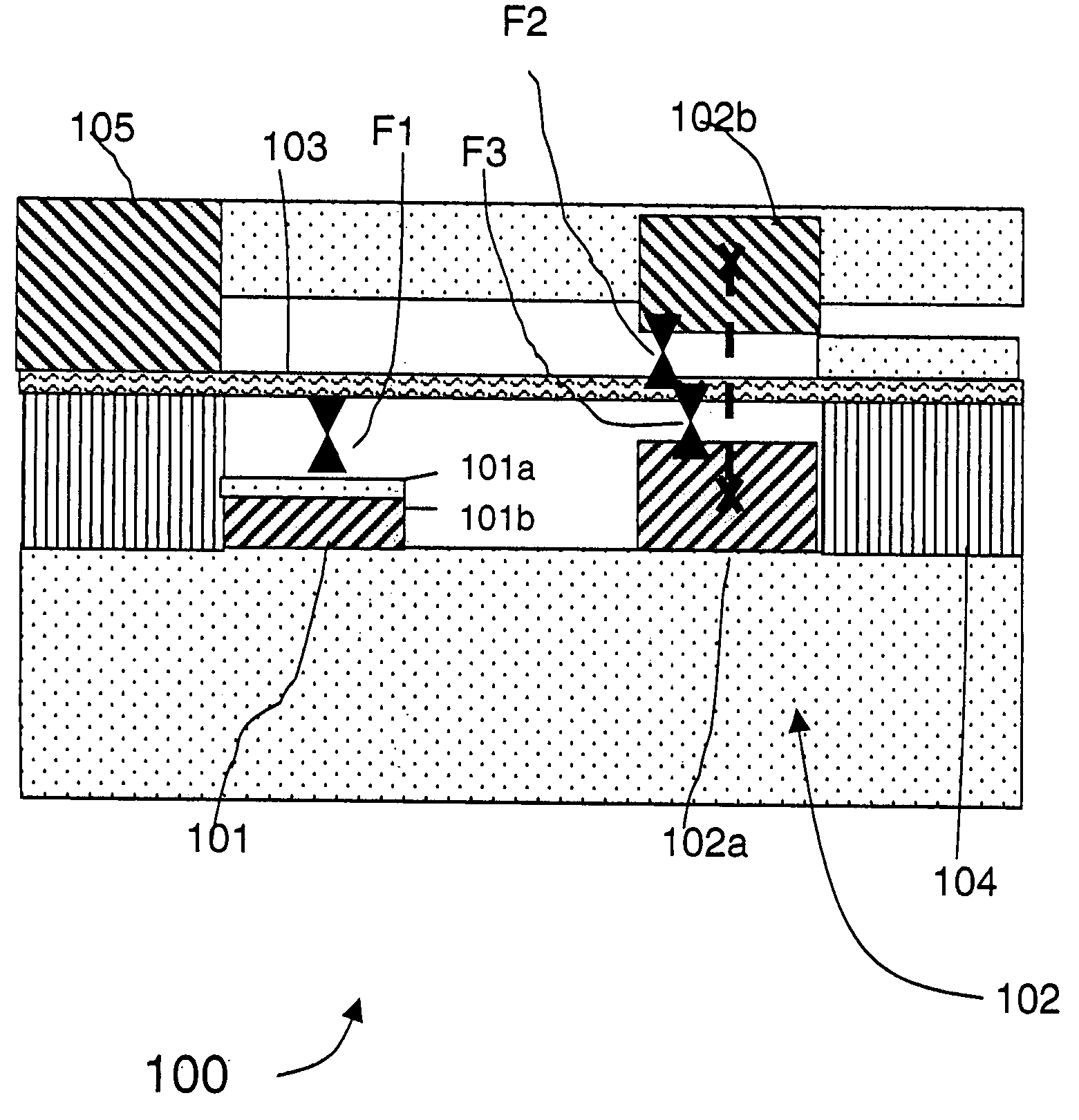
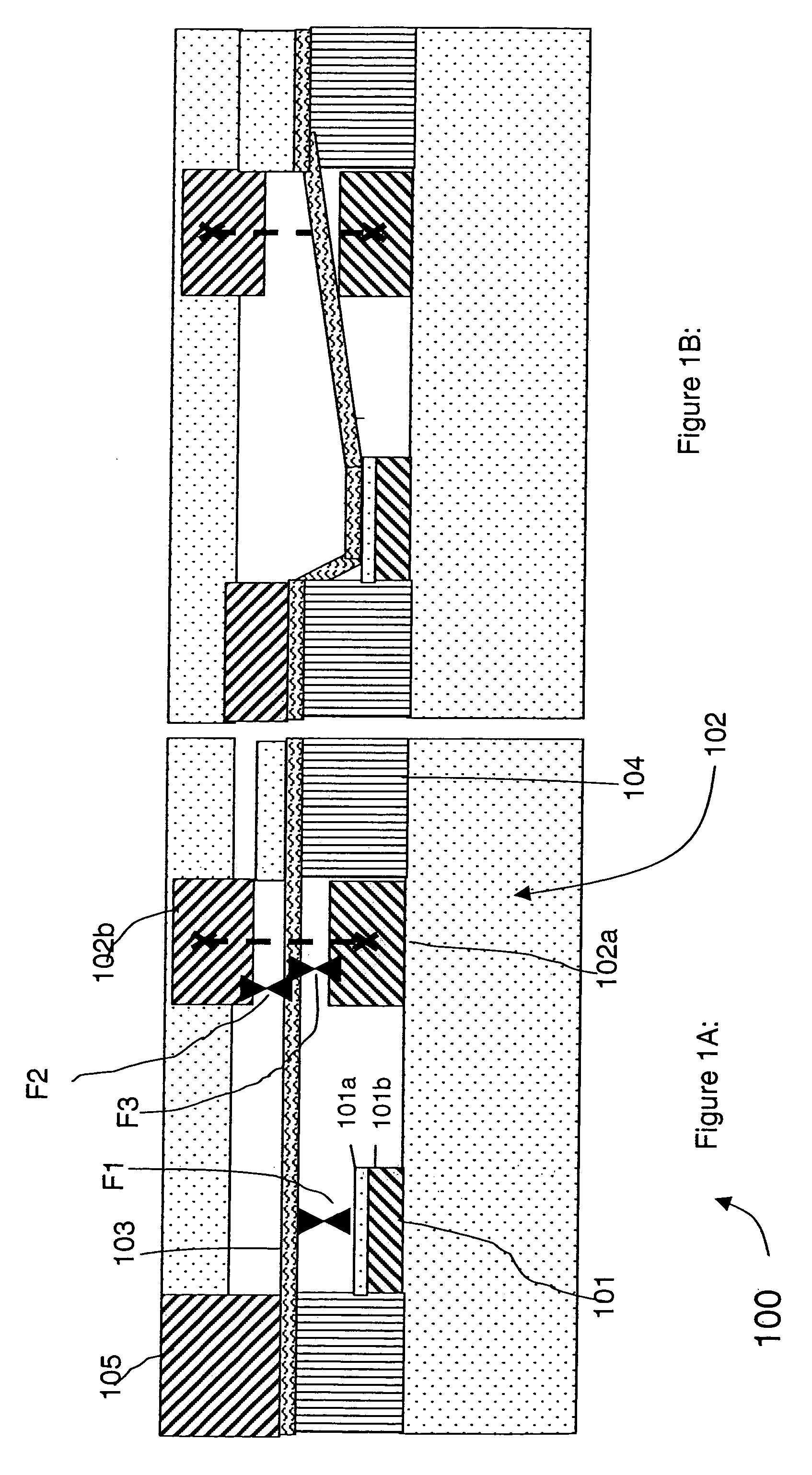
[0034] Preferred embodiments of the invention provide switching elements in which a nanotube-based channel may be controllably formed, under the influence of a control node, so that a signal may be transferred to an output node. The transferred signal may be a varying signal or a reference signal, depending on the manner in which the switching element is utilized and arranged. Preferred embodiments provide an isolation structure so that such signal transfer and the switching element's operation is substantially invariant to the output state. For example, the output node may float and / or be tied to other electrical components and the circuit will operate in a predictable switch-like manner. Consequently, the switching elements may be formed into larger circuits, such as Boolean logic circuits. Under some embodiments, the switching elements are used as complementary circuitry.

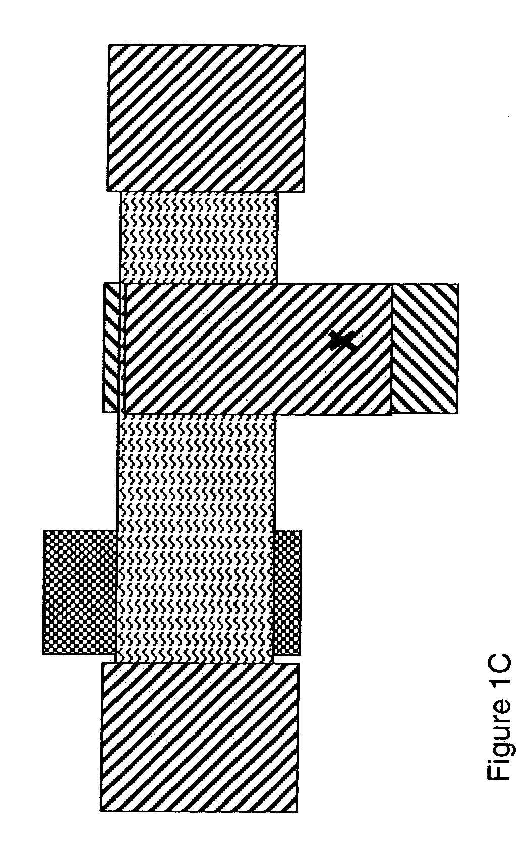
[0035]FIGS. 1A and 1B are cross-sectional views of an exemplary nanotube switching element and FIG. 1C is a l...


PUM


Abstract

Nanotube-based switching elements and logic circuits. Under one embodiment of the invention, a switching element includes an input node, an output node, a nanotube channel element having at least one electrically conductive nanotube, and a control electrode. The control electrode is disposed in relation to the nanotube channel element to controllably form an electrically conductive channel between the input node and the output node. The channel at least includes said nanotube channel element. The output node is constructed and arranged so that channel formation is substantially unaffected by the electrical state of the output node. Under another embodiment of the invention, the control electrode is arranged in relation to the nanotube channel element to form said conductive channel by causing electromechanical deflection of said nanotube channel element. Under another embodiment of the invention, the output node includes an isolation structure disposed in relation to the nanotube channel element so that channel formation is substantially invariant from the state of the output node. Under another embodiment of the invention, the isolation structure includes electrodes disposed on opposite sides of the nanotube channel element and said electrodes produce substantially the same electric field. Under another embodiment of the invention, a Boolean logic circuit includes at least one input terminal and an output terminal, and a network of nanotube switching elements electrically disposed between said at least one input terminal and said output terminal. The network of nanotube switching elements effectuates a Boolean function transformation of Boolean signals on said at least one input terminal. The Boolean function transformation includes a Boolean inversion within the function, such as a NOT or NOR function.

Description

CROSS-REFERENCE TO RELATED APPLICATIONS [0001] This application claims priority under 35 U.S.C. § 119(e) to U.S. Provisional Pat. Apl., Ser. No. 60 / 494,889, filed on Aug. 13, 2003, entitled Nanoelectromechanical Nanotube-Based Logic, which is incorporated herein by reference in its entirety. [0002] This application is related to the following references: [0003] U.S. Pat. Apl., Ser. No. not yet assigned, filed on date even herewith, entitled Nanotube-Based Switching Elements; [Nan-31][0004] U.S. Pat. Apl., Ser. No. not yet assigned, filed on date even herewith, entitled Nanotube-Based Switching Elements and Logic Circuits; [Nan-78][0005] U.S. Pat. Apl., Ser. No. not yet assigned, filed on date even herewith, entitled Nanotube-Based Switching Elements with Multiple Controls; [Nan-45][0006] U.S. Pat. Apl., Ser. No. not yet assigned, filed on date even herewith, entitled Circuits Made from Nanotube-Based Switching Elements with Multiple Controls; [Nan-80][0007] U.S. Pat. Apl., Ser. No. ...

Claims


Application Information

Patent Timeline
IPC IPC(8): G11C13/02H01H1/027H01H59/00H01L27/28H01L29/06H01L29/73H01L29/78H01L51/30
CPCB82Y10/00G11C13/025G11C23/00H01H1/0094H01H1/027H01H2001/0005H01L51/0508H01L29/0665H01L29/0673H01L29/73H01L29/78H01L51/0048H01L27/28Y10S977/943Y10S977/94H10K19/00H10K85/221H10K10/46
Inventor BERTIN, CLAUDE L.RUECKES, THOMASSEGAL, BRENT M.
Owner NANTERO
Why Eureka
Try Eureka