

Method for making a micromechanical device by removing a sacrificial layer with multiple sequential etchants
- Summary
- Abstract
- Description
- Claims
- Application Information
AI Technical Summary
Benefits of technology
Problems solved by technology
Method used
Image

Examples
Embodiment Construction
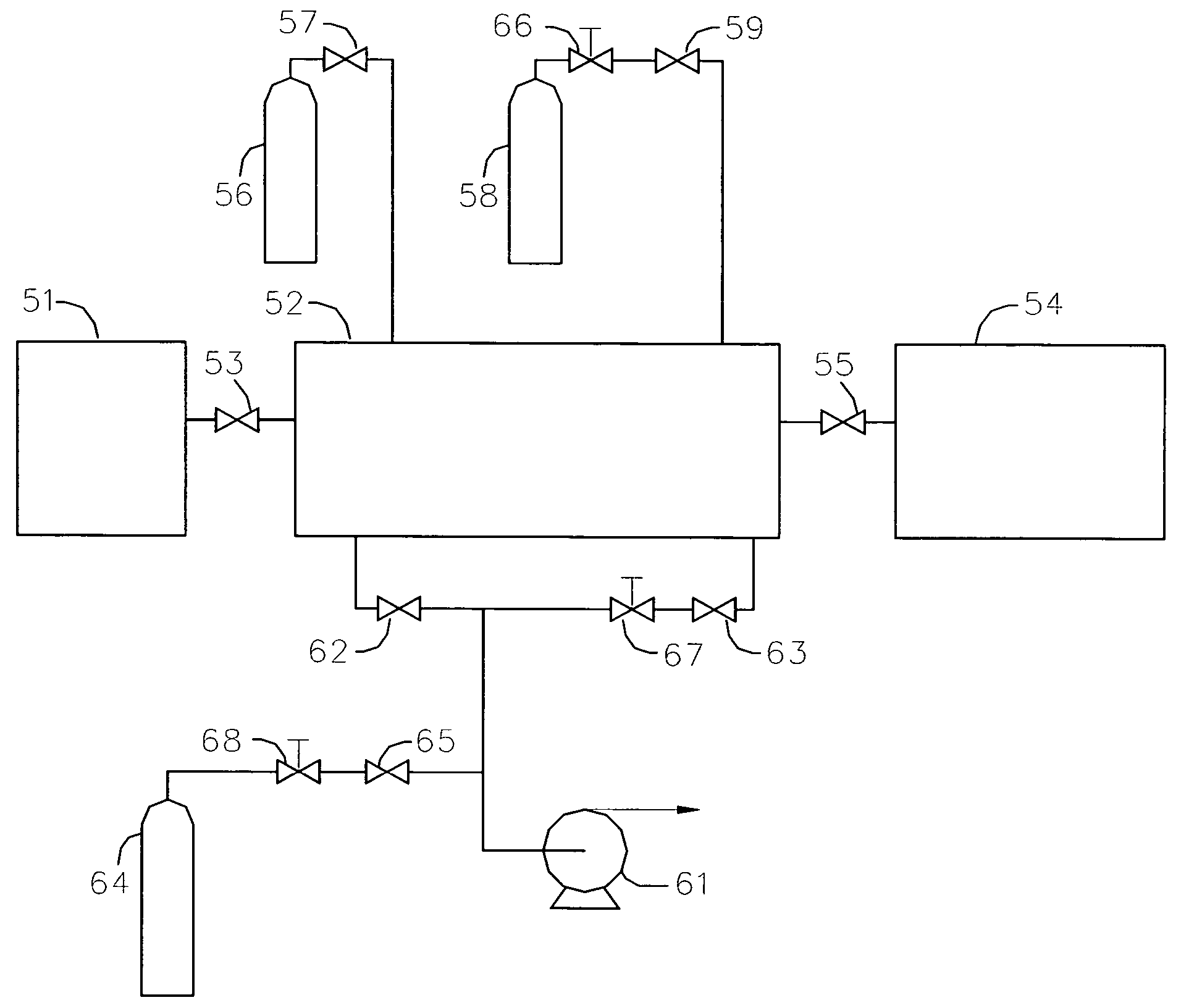
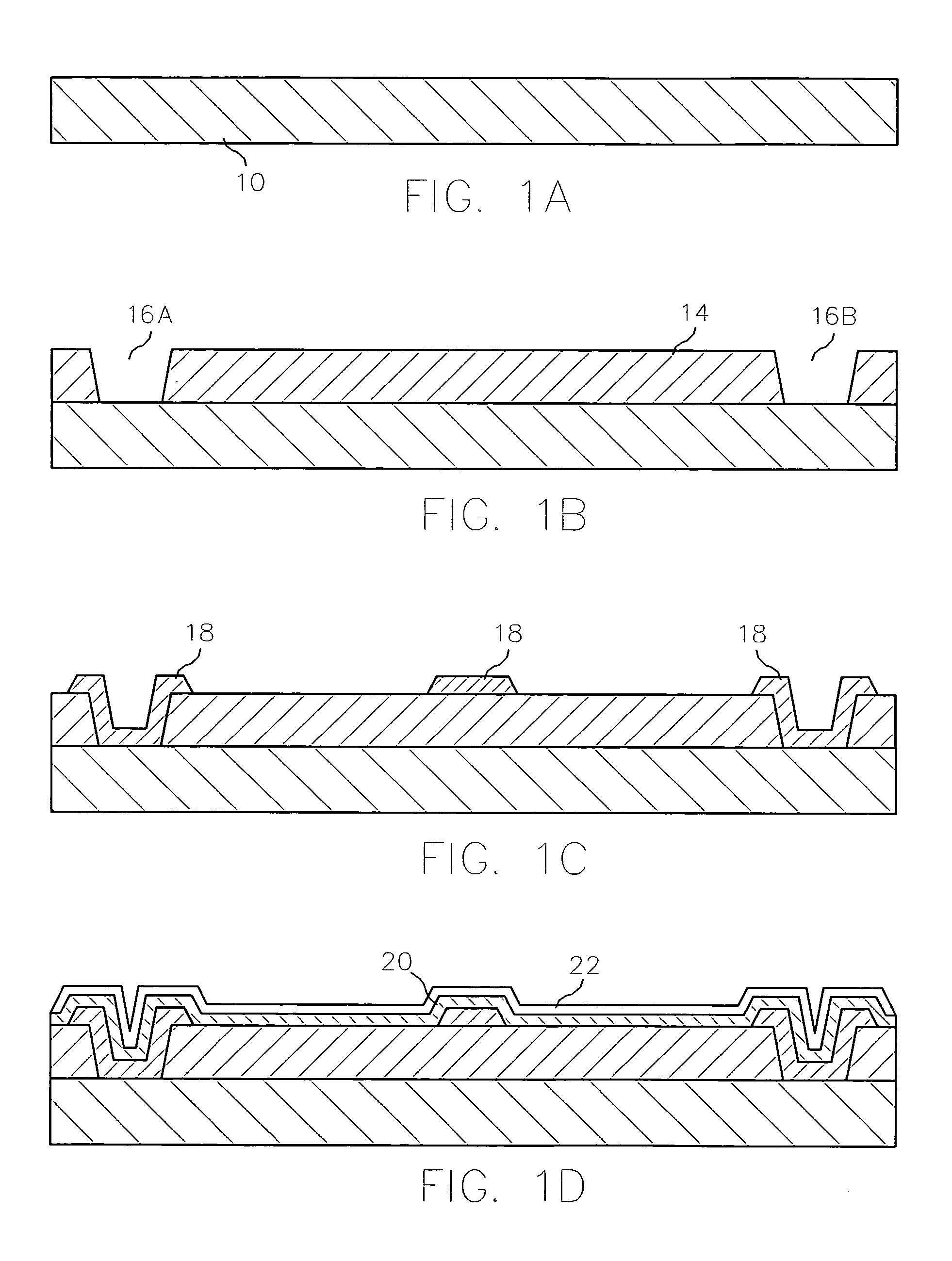
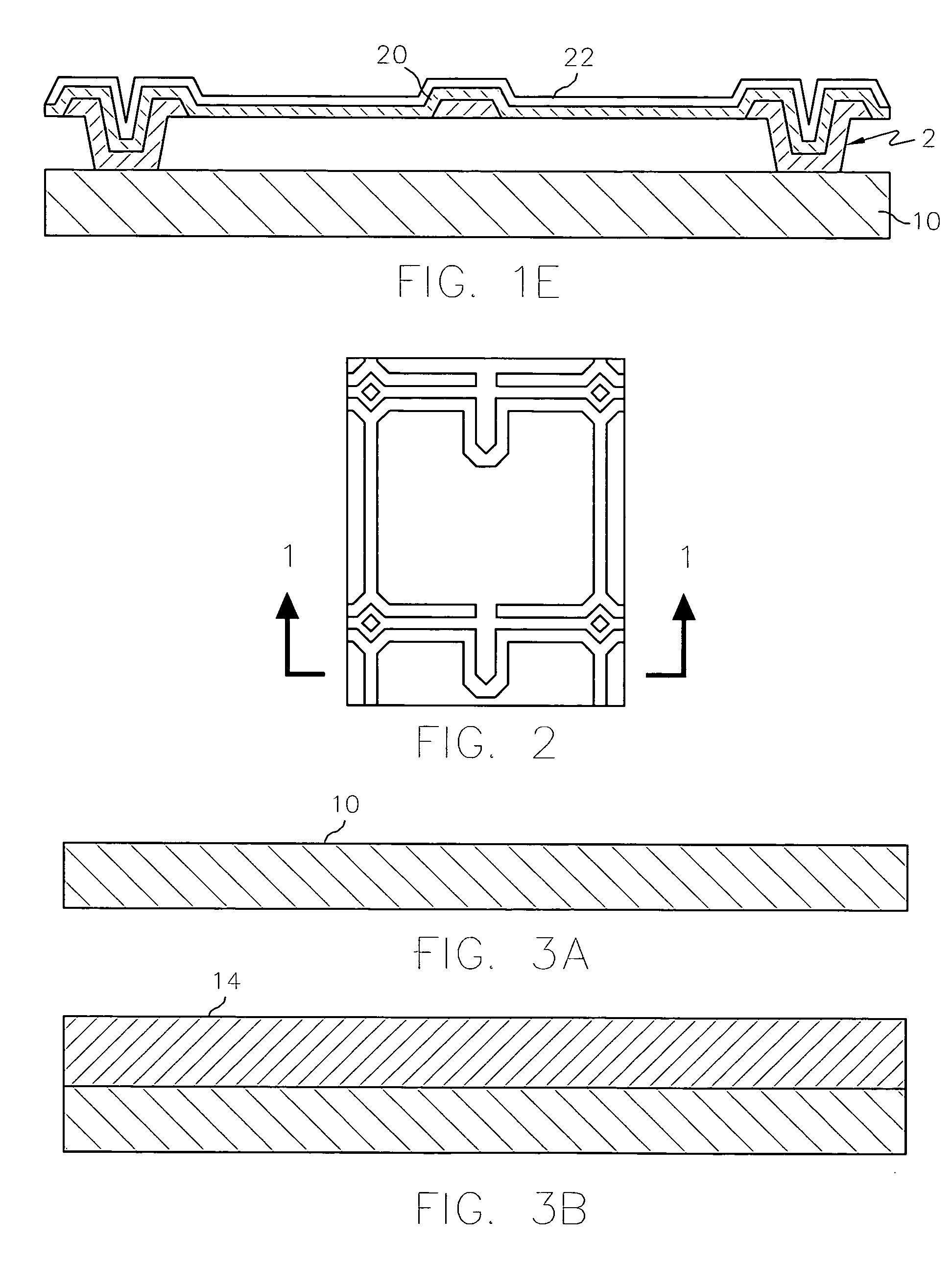
[0021] Micromechanical Structure Fabrication:
[0022] Processes for microfabricating a MEMS device such as a movable micromirror and mirror array are disclosed in U.S. Pat. Nos. 5,835,256 and 6,046,840 both to Huibers, the subject matter of each being incorporated herein by reference. A similar process for forming MEMS movable elements (e.g. mirrors) on a wafer substrate (e.g. a light transmissive substrate or a substrate comprising CMOS or other circuitry) is illustrated in FIGS. 1 to 4. By “light transmissive”, it is meant that the material will be transmissive to light at least in operation of the device (The material could temporarily have a light blocking layer on it to improve the ability to handle the substrate during manufacture, or a partial light blocking layer for decreasing light scatter during use. Regardless, a portion of the substrate, for visible light applications, is preferably transmissive to visible light during use so that light can pass into the device, be refle...
PUM
| Property | Measurement | Unit |
|---|---|---|
| Power | aaaaa | aaaaa |
| Plasma power | aaaaa | aaaaa |
Abstract
Description
Claims
Application Information