
Semiconductor device and ID generator configured as semiconductor device

a technology of semiconductor devices and semiconductor devices, applied in the field of semiconductor devices, can solve the problems of high risk of encryption information leakage, device may not function properly or be damaged, and insufficient confidentiality,

Inactive Publication Date: 2005-03-03
SANYO ELECTRIC CO LTD
View PDF6 Cites 3 Cited by
  • Summary
  • Abstract
  • Description
  • Claims
  • Application Information

AI Technical Summary

Benefits of technology

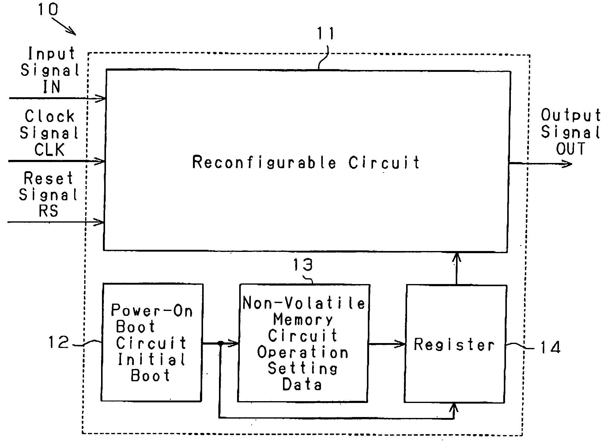
[0017] Another aspect of the invention is an ID generator, configured as a semiconductor device, for generating an identification signal required to authenticate an external device attached to a main device. The ID generator includes a reconfigurable circuit configured to dynamically respond to circuit operation setting data and generate an identification signal in accordance with predetermined encryption processing. A non-volatile memory stores the circuit operation setting data. A register is connected to the non-volatile memory and the reconfigurable circuit for receiving the circuit operation setting data when read from the non-volatile memory and providing the circuit operation setting data to the reconfigurable circuit.
[0016] A further aspect of the present invention is a semiconductor device including a plurality of signal wirings formed in a plurality of layers, respectively. A probe inhibiting wiring covers, among the plurality of signal wirings, at least a signal wiring that transmits a signal significant for analysis of operation of the semiconductor device.
[0016] A further aspect of the present invention is a semiconductor device including a plurality of signal wirings formed in a plurality of layers, respectively. A probe inhibiting wiring covers, among the plurality of signal wirings, at least a signal wiring that transmits a signal significant for analysis of operation of the semiconductor device.

Problems solved by technology

If a low-quality battery pack as such is used for a device, the device may not function properly or be damaged, for example, by the heat generated by the battery pack.
Accordingly, there is a high risk of encryption information leakage and confidentiality is not sufficient.

Method used


Image

  • Semiconductor device and ID generator configured as semiconductor device
  • Semiconductor device and ID generator configured as semiconductor device
  • Semiconductor device and ID generator configured as semiconductor device

Examples


Embodiment Construction

[0026] In the drawings, like numerals are used for like elements throughout.

[0027] A semiconductor device 10 according to a preferred embodiment of the present invention will now be described with reference to the drawings.

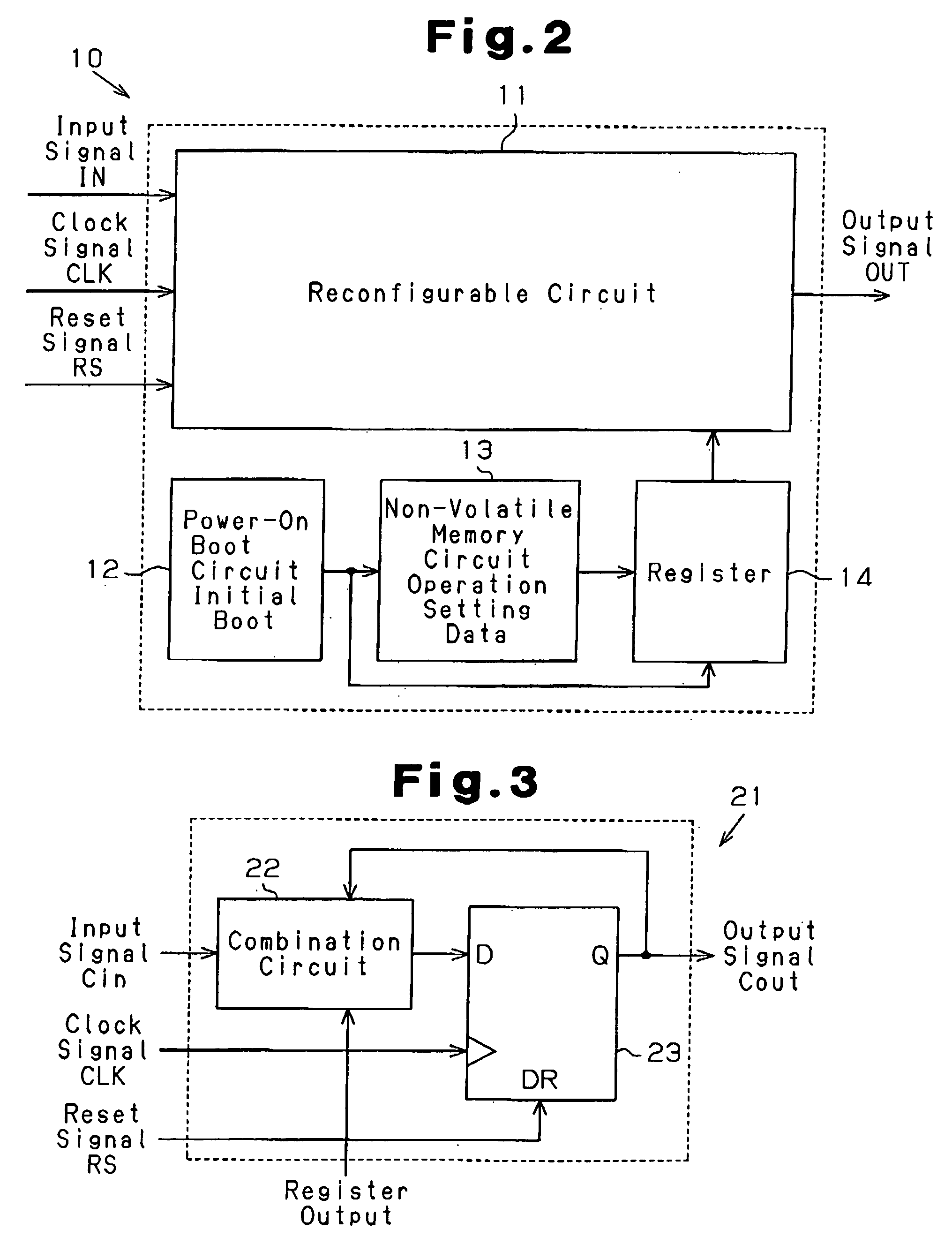
[0028] As shown in FIG. 2, the semiconductor device 10 includes a reconfigurable circuit 11, a power-on boot circuit (hereinafter referred to as “boot circuit”) 12, a non-volatile memory 13, and a register 14, all of which are formed on the same semiconductor substrate.

[0029] The reconfigurable circuit 11 includes a plurality of reconfigurable cells 21 (see FIG. 3), each of which is operation-controlled (programmed) individually. The reconfigurable circuit 11 switches circuit configurations in accordance with a combination logic set for each of the reconfigurable cells 21.

[0030] The non-volatile memory 13 stores circuit operation setting data, which is written beforehand, for setting a combination logic for each of the reconfigurable cells 21 in accordance wit...


PUM

PropertyMeasurementUnit
poweraaaaaaaaaa
mechanicalaaaaaaaaaa
structureaaaaaaaaaa

Abstract

A semiconductor device that is difficult to reverse engineer. The semiconductor device includes a reconfigurable circuit having a circuit configuration that is switchable in accordance with circuit operation setting data. A non-volatile memory stores the circuit operation setting data. A register receives the circuit operation setting data from the non-volatile memory and provides the circuit operation setting data to the reconfigurable circuit when the semiconductor device is activated. Since the circuit configuration of the reconfigurable circuit is determined by the circuit operation setting data, the operation of the reconfigurable circuit cannot be analyzed when a peeling analysis is conducted on the semiconductor device.

Description

CROSS-REFERENCE TO RELATED APPLICATIONS [0001] This application is based upon and claims the benefit of priority from prior Japanese Patent Application No. 2003-301526, filed on Aug. 26, 2003, the entire contents of which are incorporated herein by reference. BACKGROUND OF THE INVENTION [0002] The present invention relates to a semiconductor device, and more particularly, to a semiconductor device which is difficult to reverse engineer and a semiconductor device functioning as an ID generator which generates an identification signal used for identifying whether an external unit attached to a main device is authentic or not. [0003] Typically, a portable device such as a cellular phone is provided with a battery pack that is detachable from the main body. The battery pack has a battery for supplying power to the main body. If the battery deteriorates, the portable device is used continuously simply by replacing the battery pack. [0004] While various improvements have been made for red...

Claims


Application Information

Patent Timeline
Patent Type & Authority Applications(United States)
IPC IPC(8): G11C16/22H01L21/822H01L27/04H01M2/10H02J7/04H04K1/00
CPCG11C16/225H02J7/00045H01L21/822
Inventor OHKUBO, KENICHINODA, ATSUSHI
Owner SANYO ELECTRIC CO LTD
Learn More