Method of manufacturing semiconductor element

a manufacturing method and semiconductor technology, applied in the direction of basic electric elements, semiconductor devices, electrical equipment, etc., can solve the problems of unable to use the sheet, traces of work damage from laser irradiation can be found on the surface of the wafer, etc., and achieve the effect of stably activating in a short tim

Active Publication Date: 2005-03-17
FUJI ELECTRIC CO LTD
View PDF5 Cites 39 Cited by
  • Summary
  • Abstract
  • Description
  • Claims
  • Application Information

AI Technical Summary

Benefits of technology

[0034] It is an object of the present invention to provide a method of manufacturing a semiconductor element which can stably activate...

Problems solved by technology

However, an alternating current input requires a semiconductor switch to have a high reverse breakdown voltage.
Furthermore, in the method of using an adhesive sheet for preventing cracking of wafer, the permissible temperature of the adhesive sheet being usually 200° C. or less makes the use of t...

Method used


Image

  • Method of manufacturing semiconductor element
  • Method of manufacturing semiconductor element
  • Method of manufacturing semiconductor element

Examples


Embodiment Construction

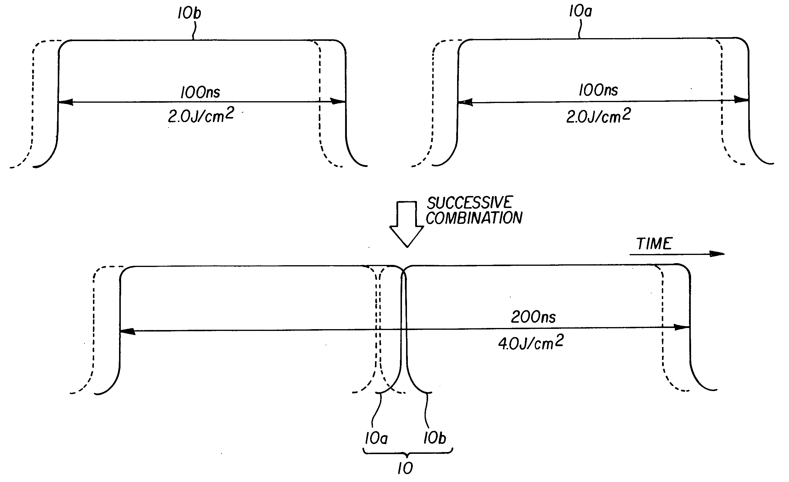
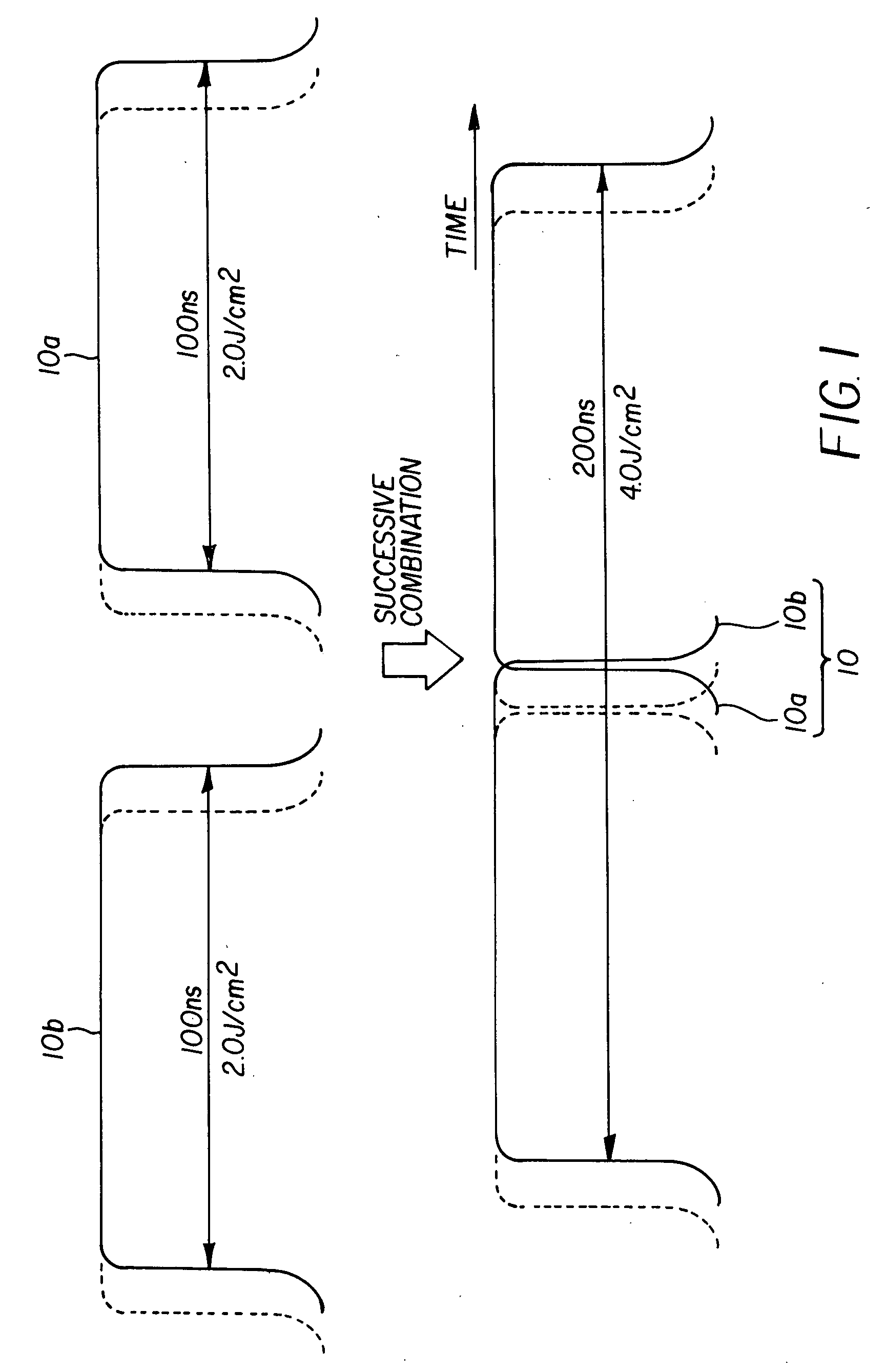
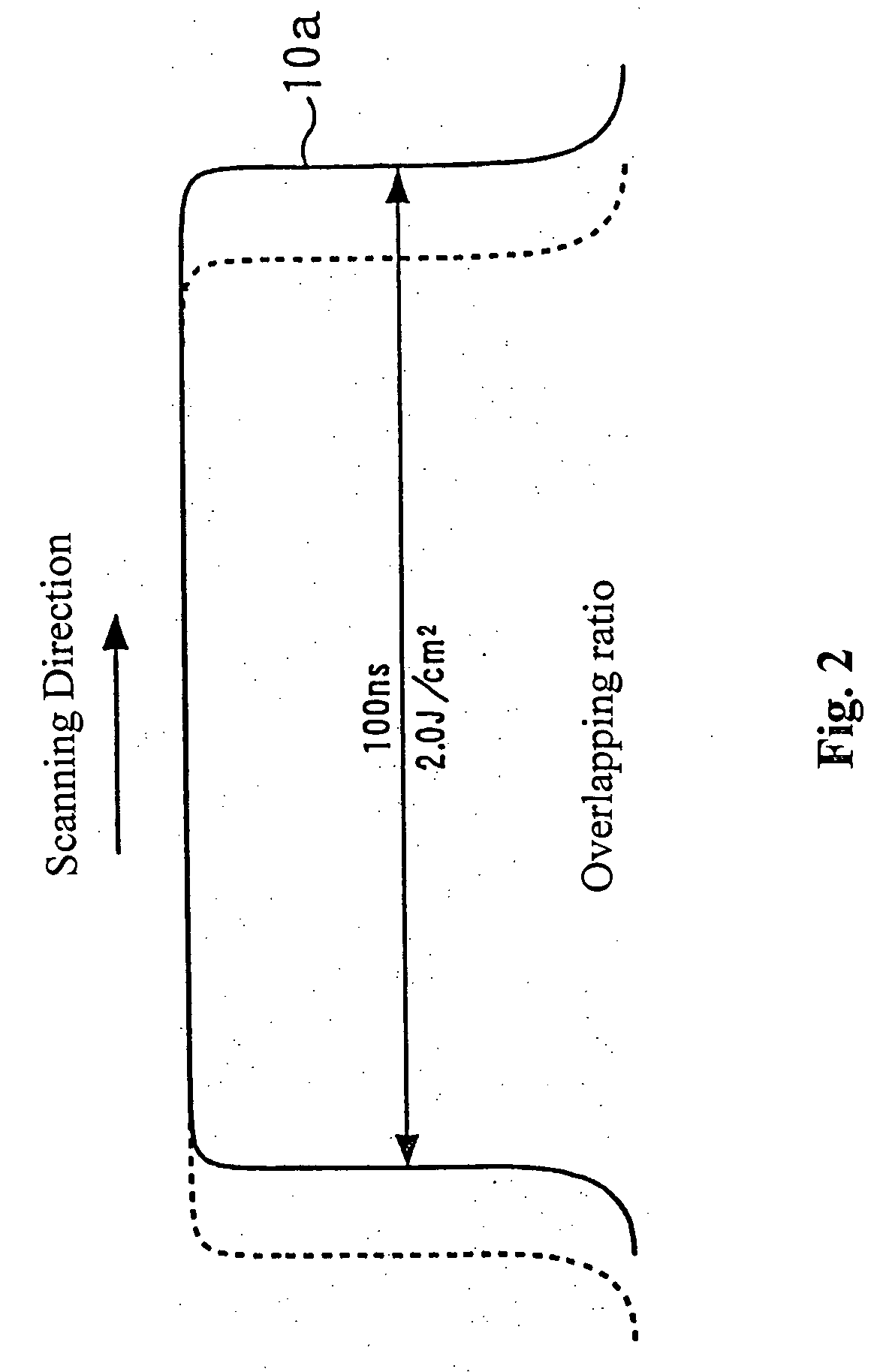
[0083] A plurality of laser irradiation devices is used according to the present invention to laser activate a doped layer region. The doped layer region in an irradiation area is successively irradiated with a plurality of pulsed beams being projected from the respective laser irradiation devices in order to activate the doped layer region. The effect is the same as that obtained by irradiating the doped layer region with a single pulsed beam having a long full-width at half maximum to enable a high rate of activation from a shallow region to a deep region of the doped layer region. Therefore, a semiconductor element having a p-layer or an n-layer as the doped layer region and a semiconductor element having successive doped layers such as pn-successive layers as a doped layer region can be stably activated in a short time, on the order of nanoseconds, to make it possible to manufacture semiconductor elements having superior device characteristics.

[0084] In the following, modes for...


PUM


Abstract

A method for stably activating pn-successive layers in a semiconductor element in a short time is disclosed. Pulsed beams, each of which has a pulse shape that is approximately rectangular, are projected from respective laser irradiation devices and successively combined into a pulsed beam equivalent to one pulse, with which the doped layer region is irradiated. By successively projecting the pulsed beams onto the doped layer region in this way, an effect is obtained which is the same as that of irradiating the doped layer region with a single pulsed beam having a long full-width at half maximum. A high activation ratio from a shallow region to a deep region of the doped layer region is enabled. This can stably activate the semiconductor element having the pn-successive layers as the doped layer region in a short time, making possible the manufacture of semiconductor elements having superior device characteristics.

Description

CROSS REFERENCE TO RELATED APPLICATIONS [0001] This application claims priority from application Serial No. JP 2003-179725 filed on Jun. 23, 2003 and JP 2004-001670, filed on Jan. 7, 2004, and the contents of these two documents are incorporated herein by reference in their entirety. BACKGROUND OF THE INVENTION [0002] A. Field of the Invention [0003] The present invention relates to a method of manufacturing a semiconductor element, and more particularly to a method of manufacturing a semiconductor element such as an IC (integrated circuit), a MOS (metal oxide semiconductor) or an insulated gate bipolar transistor (hereinafter referred to as an “IGBT”). [0004] B. Description of the Related Art [0005] In recent years, integrated circuits (ICs) have been most commonly used in important sections in a computer or a communication device. In such ICs, a number of transistors and resistors are connected so as to form electric circuits that are integrated onto one chip. Of these ICs, those ...

Claims


Application Information

Patent Timeline
IPC IPC(8): H01L21/268H01L21/331
CPCH01L29/66325H01L21/268
Inventor NAKAZAWA, HARUOKIRISAWA, MITSUAKISHIMOYAMA, KAZUO
Owner FUJI ELECTRIC CO LTD
Why Eureka
Try Eureka