Structure and method of making sealed capped chips

a technology of sealed caps and chips, applied in the field of microelectronic packaging, can solve the problems of requiring a relatively complex series of steps for forming terminals on caps, requiring a relatively complex series of steps, and providing terminals for mems devices

Inactive Publication Date: 2005-04-21
TESSERA INC
View PDF67 Cites 121 Cited by
  • Summary
  • Abstract
  • Description
  • Claims
  • Application Information

AI Technical Summary

Problems solved by technology

This increases the area of the active wafer required to form each unit, requires additional operations and results in an assembly considerably larger than the unit itself.
However, formation of terminals on the caps and vias for connecting the terminals to the contacts on the active wafer requires a relatively complex series of steps.
Similar problems occur in providing terminals for MEMS devices.

Method used


Image

  • Structure and method of making sealed capped chips
  • Structure and method of making sealed capped chips
  • Structure and method of making sealed capped chips

Examples


Embodiment Construction

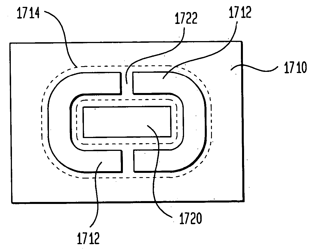
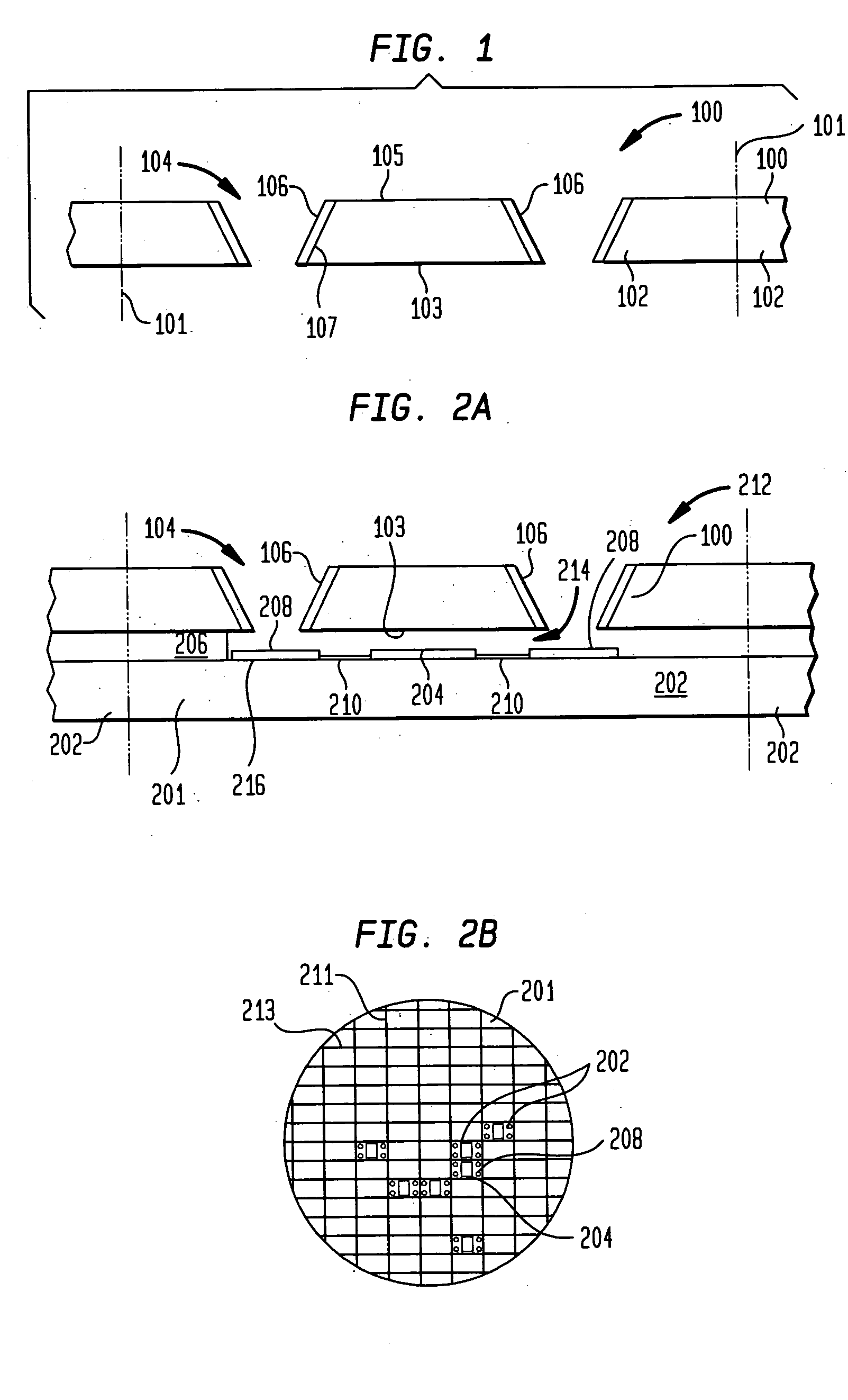
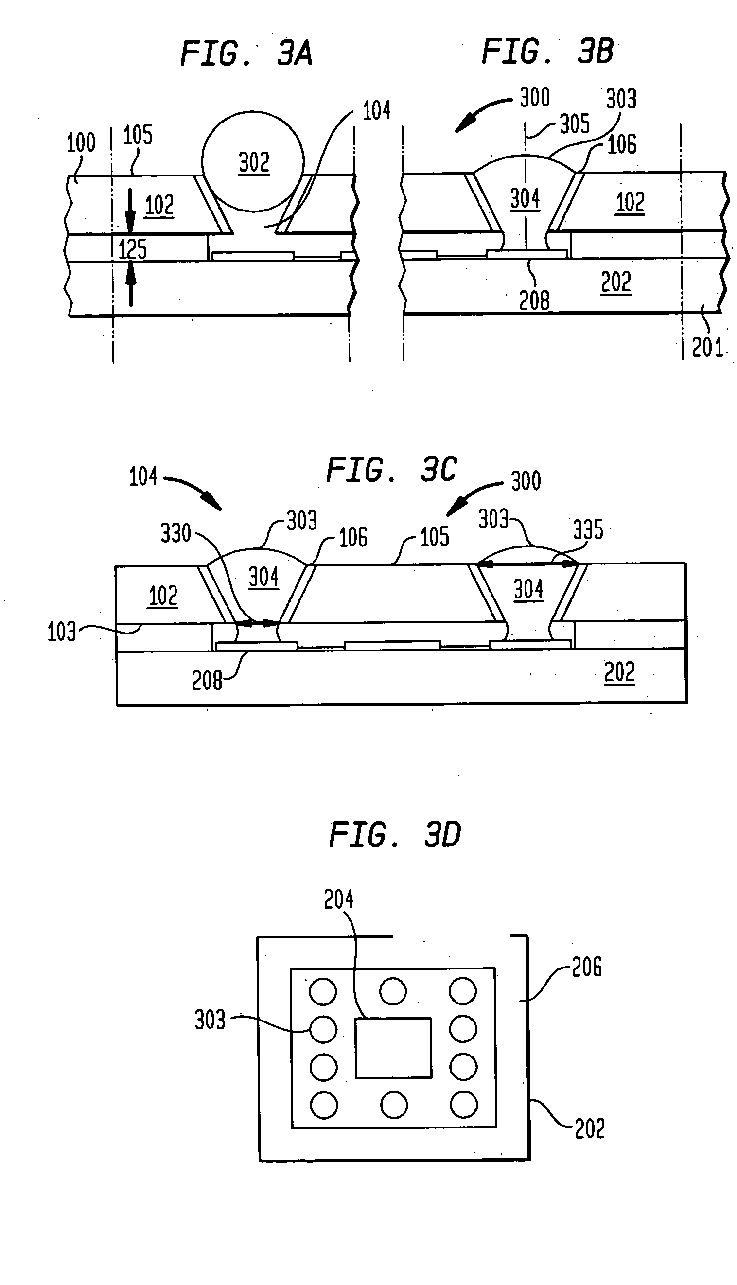
[0152]FIGS. 1-3D illustrated a capped chip and stages in a method for fabricating a capped chip according to an embodiment of the invention. In particular, FIG. 3C is a sectional view illustrating a capped chip 200 and FIG. 3D is a plan view illustrating the interconnects and the seal provided on the surface of a chip included in the capped chip.

[0153] Particular types of devices, such as SAW devices and MEMs need to be sealed hermetically in order to function appropriately over the life of the device. For many silicon semiconductor devices, a package is considered to be hermitic if it has a leak rate of helium below 1×10⁻⁸ Pa m3 / sec. Other devices such as electro-optical devices do not require hermeticity, but nevertheless are best packaged under a protective lid, e.g., one that is optically transmissive, as a way of preventing particles from reaching a surface of the electro-optic device.

[0154] In a method of forming the capped chips, a plurality of caps 102, e.g., as contained ...


PUM


Abstract

A method of making a plurality of sealed assemblies is provided which includes a) assembling a first element to a second element so that a bottom surface of the first element faces downwardly toward a front surface of the second element and a top surface of the first element faces upwardly away from the second element; and (b) forming ring seals surrounding regions of the front surface of the second element by introducing flowable material between the first element and the second element from the top surface of the first element through openings in the first element. A chip is provided which includes: (a) a body defining a front surface and one or more circuit elements on or within the body; (b) one or more bond pads exposed at the front surface in a bond pad region; and (c) a metallic ring exposed at the front surface, the ring substantially surrounding the bond pad region. Sealed chip assemblies are formed by sealing an array of the chips, e.g., in wafer form, to a cap element.

Description

[0001] This application claims the benefit of the filing dates of U.S. Provisional Patent Application Nos. 60 / 506,500 filed Sep. 26, 2003, 60 / 515,615 filed Oct. 29, 2003, 60 / 532,341 filed Dec. 23, 2003, 60 / 568,041 filed May 4, 2004, 60 / 574,523 filed May 26, 2004, and is a continuation-in-part of U.S. patent application Ser. No. 10 / 928,839, filed Aug. 27, 2004 entitled PACKAGE HAVING INTEGRAL LENS AND WAFER SCALE FABRICATION METHOD THEREFOR, on which Catherine De Villeneuve, Giles Humpston, and David B. Tuckerman are named inventors, the disclosures of all such applications being hereby incorporated herein by reference.BACKGROUND OF THE INVENTION [0002] The present invention relates to microelectronic packaging. Microelectronic chips typically are thin, flat bodies with oppositely facing, generally planar front and rear surfaces and with edges extending between these surfaces. Chips generally have contacts on the front surface, which are electrically connected to the circuits within ...

Claims


Application Information

Patent Timeline
Patent Type & Authority Applications(United States)
IPC IPC(8): H01L21/60H01L23/04H01L23/10H01L23/485H01L27/146H03H3/007H03H3/08H03H9/10
CPCB81B2207/095B81C1/00293B81C1/00301B81C2203/0118B81C2203/019H01L21/76898H01L23/04H01L23/3114H01L24/48H01L27/14618H01L27/14627H01L27/14636H01L33/62H01L2224/0401H01L2224/13099H01L2224/131H01L2224/13124H01L2224/13139H01L2224/13144H01L2224/13147H01L2224/13169H01L2224/16H01L2224/48091H01L2224/48227H01L2224/48228H01L2224/4824H01L2224/48247H01L2224/484H01L2224/81801H01L2924/01002H01L2924/01003H01L2924/01005H01L2924/01006H01L2924/01013H01L2924/01014H01L2924/01018H01L2924/01022H01L2924/01027H01L2924/01028H01L2924/01029H01L2924/0103H01L2924/01042H01L2924/01046H01L2924/01047H01L2924/0105H01L2924/01058H01L2924/01061H01L2924/01077H01L2924/01078H01L2924/01079H01L2924/01082H01L2924/01322H01L2924/014H01L2924/04941H01L2924/09701H01L2924/12044H01L2924/14H01L2924/15153H01L2924/15165H01L2924/15311H01L2924/16151H01L2924/16195H01L2924/16235H01L2924/3011H01L2924/3025H03H3/007H03H9/0547H03H9/0585H03H9/059H03H9/1057H03H9/1064H03H9/1071H01L2924/01023H01L2924/01024H01L2924/01033B81C2203/0145H01L2924/10253H01L24/11H01L24/13H01L2224/11334H01L2224/1401H01L2924/07811H01L2924/1461H01L2924/00014H01L2924/00H01L2924/00012H01L24/24H01L24/82H01L2224/05624H01L2224/05644H01L2224/06135H01L2224/11H01L2224/13H01L2224/82101H01L2224/9202H01L2924/12042H01L2924/15787H01L2224/45099
Inventor MCWILLIAMS, BRUCE M.HUMPSTON, GILESHABA, BELGACEMTUCKERMAN, DAVID B.
Owner TESSERA INC
Why Eureka
Try Eureka