Plasma display panel

a technology of display panel and plasma, which is applied in the direction of gas discharge vessel/container, electrode, gas-filled discharge tube, etc., can solve the problems of large influence of electrodes on discharge efficiency, poor illumination efficiency, and significant reduction of overall panel efficiency (i.e., brightness ratio), so as to improve screen brightness and discharge efficiency

Inactive Publication Date: 2005-04-28
SAMSUNG SDI CO LTD
View PDF5 Cites 21 Cited by
  • Summary
  • Abstract
  • Description
  • Claims
  • Application Information

AI Technical Summary

Benefits of technology

[0010] In one exemplary embodiment of the present invention, there is provided a plasma display panel in which the f

Problems solved by technology

Therefore, the formation of the sustain electrodes greatly affects discharge efficiency.
However, this is generally not the case, and it is common practice to form the barrier ribs and sustain electrodes with the goal of simplifying design and manufacture.
This often results in poor illumination efficiency.
That is, if t

Method used


Image

  • Plasma display panel
  • Plasma display panel
  • Plasma display panel

Examples


Embodiment Construction

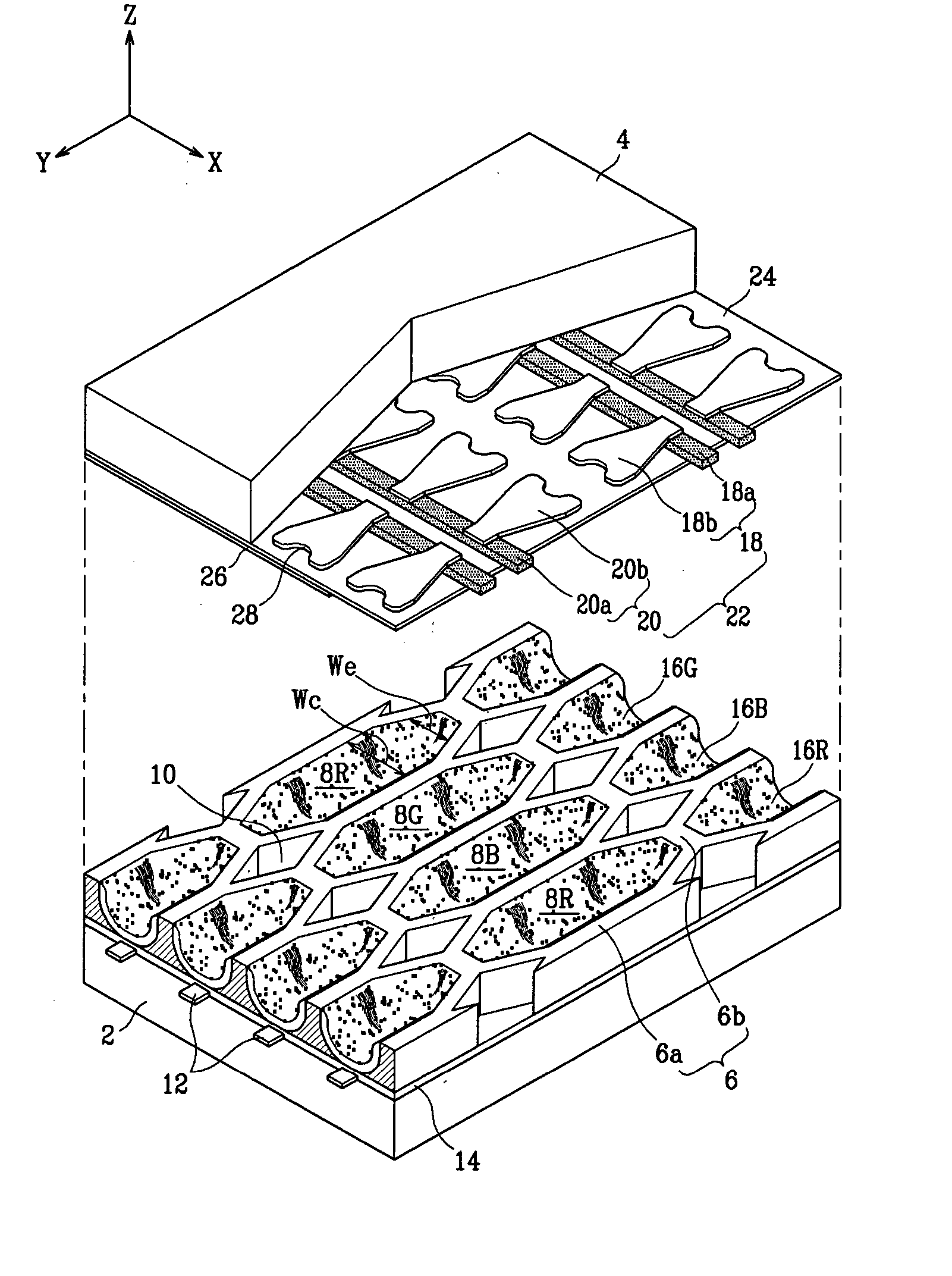
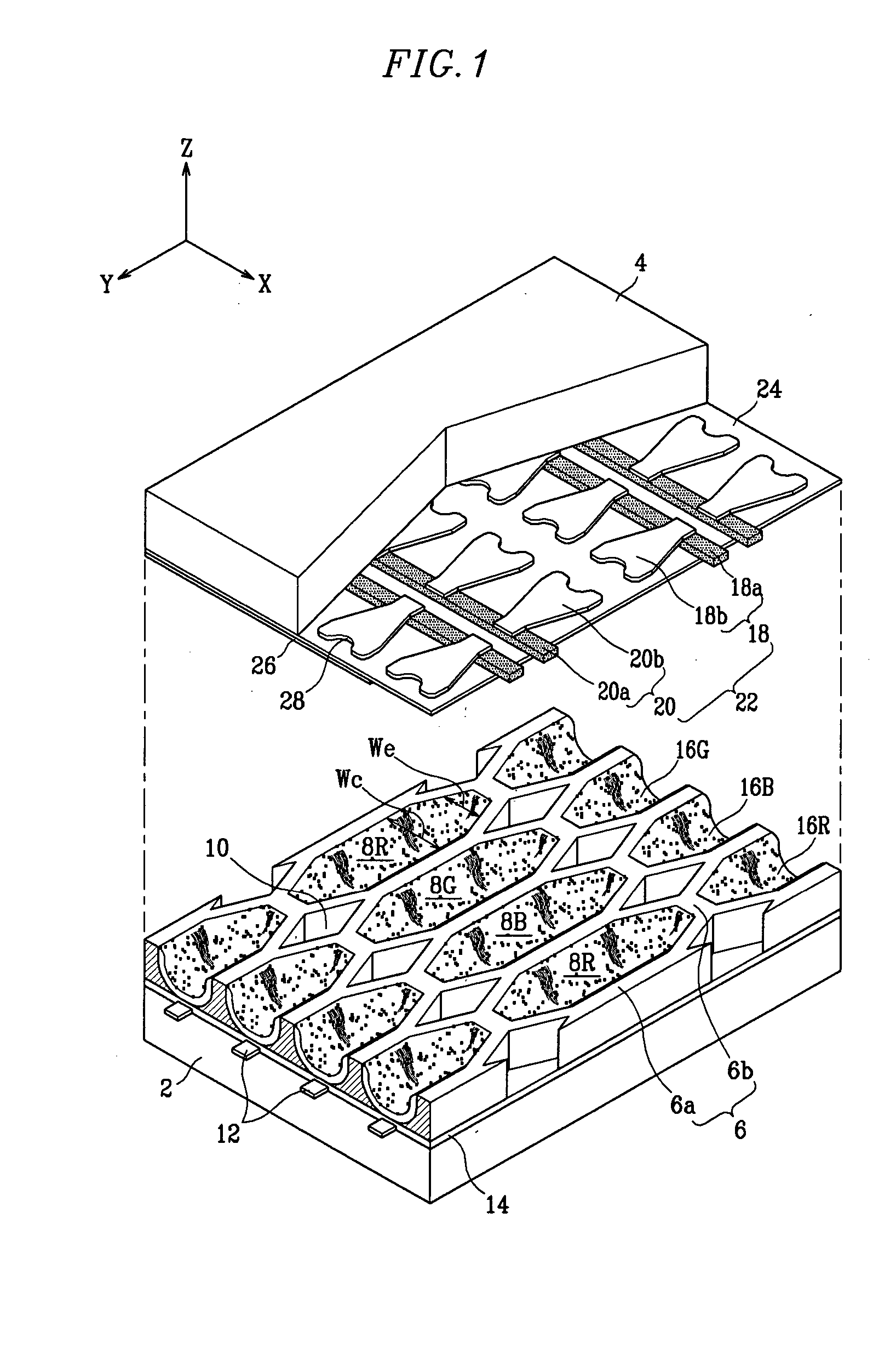
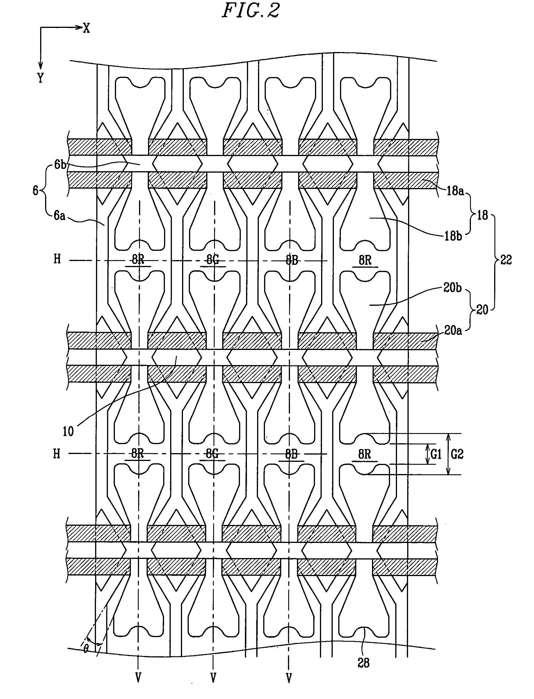
[0026] Referring to FIGS. 1-3, in the PDP of an exemplary embodiment of the present invention, first substrate 2 and second substrate 4 are provided opposing one another with a predetermined gap therebetween. Non-discharge regions 10 and discharge cells 8R, 8G, 8B are defined by barrier ribs 6 in the gap between the first and second substrates 2, 4.

[0027] Address electrodes 12 are formed on an inner surface of first substrate 2 opposing second substrate 4. Address electrodes 12 are formed along one direction (direction Y). As an example, address electrodes 12 are formed in a striped pattern with predetermined spacing between adjacent address electrodes 12. First dielectric layer 14 is formed over an entire inner surface of first substrate 2 covering address electrodes 12.

[0028] Barrier ribs 6 are formed on first dielectric layer 14. Barrier ribs 6 define non-discharge regions 10 and discharge cells 8R, 8G, 8B as described above. Discharge cells 8R, 8G, 8B are spaces where gas disc...


PUM


Abstract

A plasma display panel includes first and second substrates opposing one another. Address electrodes are formed on the first substrate in a first direction. Barrier ribs are mounted between the first and second substrates defining non-discharge regions and discharge cells, and phosphor layers are formed within the discharge cells. Discharge sustain electrodes are formed on the second substrate in a second direction substantially perpendicular to the first direction. The non-discharge regions are formed in areas encompassed by discharge cell abscissas and ordinates that pass through centers of adjacent discharge cells. The discharge sustain electrodes include bus electrodes that extend such that a pair of the bus electrodes is provided for each of the discharge cells, and protrusion electrodes formed extending from each of the bus electrodes such that a pair of opposing protrusion electrodes is formed in each discharge cell. Also, a predetermined angle is formed between proximal ends of the protrusion electrodes and inner surfaces of the barrier ribs opposing the proximal ends.

Description

CROSS-REFERENCE TO RELATED APPLICATION [0001] This application claims priority to and the benefit of Korean Patent Application No. 10-2003-0074272, filed on Oct. 23, 2003 in the Korean Intellectual Property Office, the entire content of which is incorporated herein by reference. BACKGROUND OF THE INVENTION [0002] (a) Field of the Invention [0003] The present invention relates to a plasma display panel (PDP), and more particularly, to a PDP in which the formation of discharge sustain electrodes is optimized. [0004] (b) Description of the Related Art [0005] A PDP is typically a display device in which ultraviolet rays generated by the discharge of gas excite phosphors to realize predetermined images. With its ability to realize high-resolution images, the PDP is emerging as one of the most popular flat panel display configurations used for wall-mounted televisions and other similar large-screen applications. [0006] In the conventional triode surface discharge AC-PDP, address electrode...

Claims


Application Information

Patent Timeline
IPC IPC(8): H01J11/12H01J11/22H01J11/24H01J11/26H01J11/34H01J11/36
CPCH01J11/12H01J11/32H01J2211/365H01J2211/326H01J2211/245H01J11/24H01J11/36
Inventor KIM, SE-JONGWOO, SEOK-GYUN
Owner SAMSUNG SDI CO LTD
Why Eureka
Try Eureka