Methods adapted for use in semiconductor processing apparatus including electrostatic chuck

Inactive Publication Date: 2006-04-27
SAMSUNG ELECTRONICS CO LTD +1
View PDF11 Cites 19 Cited by
  • Summary
  • Abstract
  • Description
  • Claims
  • Application Information

AI Technical Summary

Benefits of technology

[0018] One embodiment of the invention provides a plasma processing method for use in a plasma processing apparatus capable

Problems solved by technology

However currently, wet etching is rarely used because it is highly isotropic and therefore not well suited to the manufacture of highly integrated devices.
Unfortunately, a number of problems are commonly encountered when securing a wafer in the conventional plasma etching apparatus.
For example, the mechanical clamp used to secure the wafer may expose the wafer to foreign substances, i.e., contaminants that may cause defects in the wafer.
In addition, helium gas applied to the ESC to cool the wafer may cause the wafer to float over the ESC.
However, where the de-chucking operation is incompletely or incorrectly performed, the wafer may be damaged or displaced from its proper position due to popping or sticking when it is unloaded by a lift pin.
Unfortunately, however, where the wafer has a high permitt

Method used


Image

  • Methods adapted for use in semiconductor processing apparatus including electrostatic chuck
  • Methods adapted for use in semiconductor processing apparatus including electrostatic chuck
  • Methods adapted for use in semiconductor processing apparatus including electrostatic chuck

Examples


Example

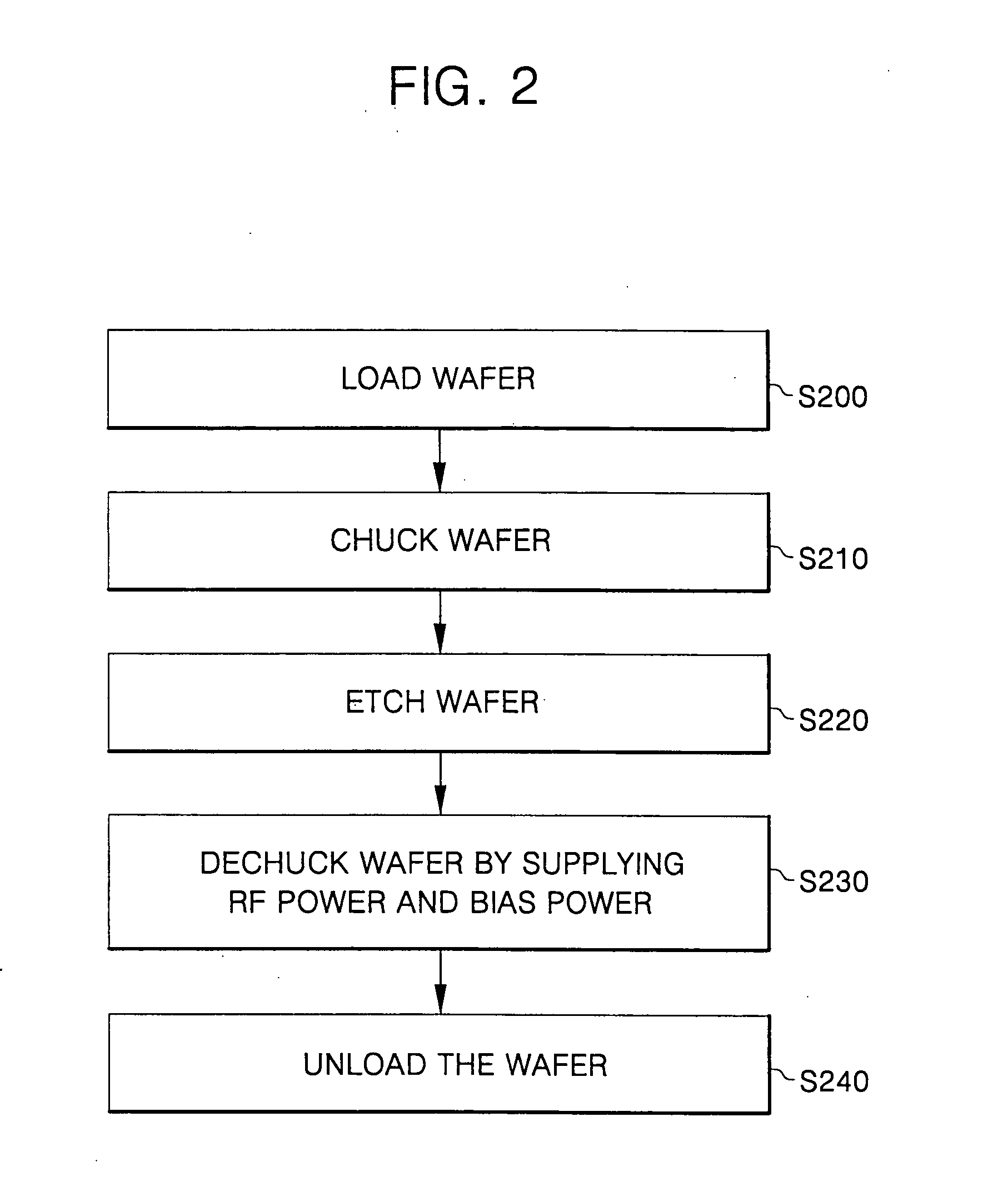
[0031] Exemplary embodiments of the invention are described below with reference to the corresponding drawings. These embodiments are presented as teaching examples. The actual scope of the invention is defined by the claims that follow.

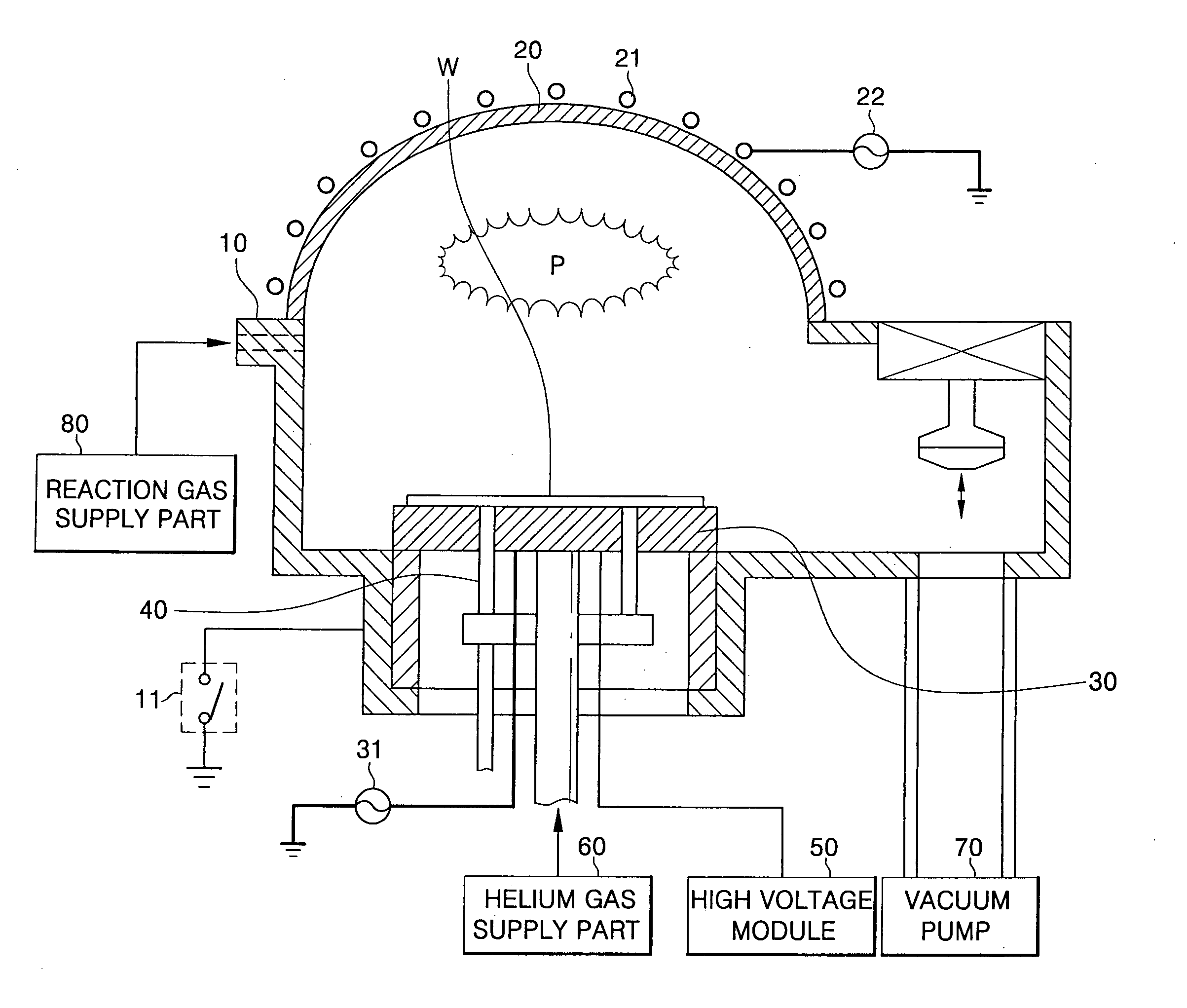
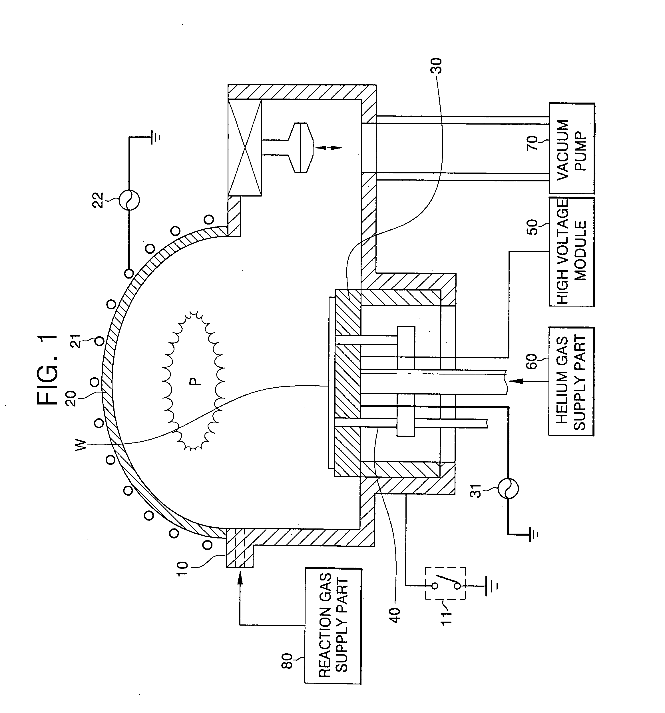
[0032] Methods of controlling a semiconductor manufacturing apparatus in accordance embodiments of the present invention are described below with reference to a plasma etching apparatus shown in FIG. 1. The plasma etching apparatus of FIG. 1 is an inductively coupled plasma (ICP) etching apparatus, however the methods find ready application in other plasma etching apparatuses as well. Moreover, the methods also find application in other (non plasma etching) semiconductor manufacturing apparatuses using an ESC, such a chemical vapor deposition (CVD) apparatus.

[0033] Referring to FIG. 1, the plasma etching apparatus includes a chamber 10, a ceramic dome shaped cover 20 installed on the chamber, and a discharge switch 11 connected between the chamber ...


PUM


Abstract

A method of controlling a plasma etching apparatus comprises loading a wafer into a chamber containing an electrostatic chuck, securing the wafer to the electrostatic chuck, performing a process on the wafer, removing the wafer from the electrostatic chuck, and unloading the wafer from the chamber. The wafer is secured to the electrostatic chuck by applying a high voltage to the electrostatic chuck. The wafer is removed from the electrostatic chuck by disconnecting the high voltage from the electrostatic chuck, applying radio frequency power to the chamber to generate a de-chucking plasma from a reaction gas in the chamber, and applying bias power to the electrostatic chuck to increase the energy of ions in the de-chucking plasma, thereby removing excess electrical charges from the wafer.

Description

BACKGROUND OF THE INVENTION [0001] 1. Field of the Invention [0002] The invention relates generally to methods adapted for use in a semiconductor processing apparatus including an electrostatic chuck. More particularly, the invention relates to methods of transferring a wafer to and from an electrostatic chuck in a plasma etching apparatus. [0003] A claim of priority is made to Korean Patent Application No. 2004-84582 filed Oct. 21, 2004, the disclosure of which is hereby incorporated by reference in its entirety. [0004] 2. Description of the Related Art [0005] Semiconductor devices are typically manufactured through some form of etching. Etching is a subtractive process whereby portions of a material layer or layers are removed from a substrate to form patterns on the substrate. The portions of the material layer(s) are usually removed by dissolving them in liquid chemicals or by converting them into a gaseous compound. Etching techniques involving chemicals in liquid phase are col...

Claims


Application Information

Patent Timeline
IPC IPC(8): H01T23/00
CPCH01J37/321H01L21/67069H01L21/6831H01L21/3065
Inventor KIM, TAEG-KONCHOI, JAE-SUNJUNG, YOON-SANG
Owner SAMSUNG ELECTRONICS CO LTD
Why Eureka
Try Eureka