Light emitting or light receiving semiconductor module and method for manufacturing same
a technology of semiconductor modules and semiconductor modules, which is applied in the direction of semiconductor devices for light sources, semiconductor devices for lighting and heating apparatus, and planar light sources. it can solve the problems of difficult manufacturing large semiconductor modules, difficulty in obtaining surrounding reflected and scattered light, and increased manufacturing costs
- Summary
- Abstract
- Description
- Claims
- Application Information
AI Technical Summary
Problems solved by technology
Method used
Image

Examples
first embodiment
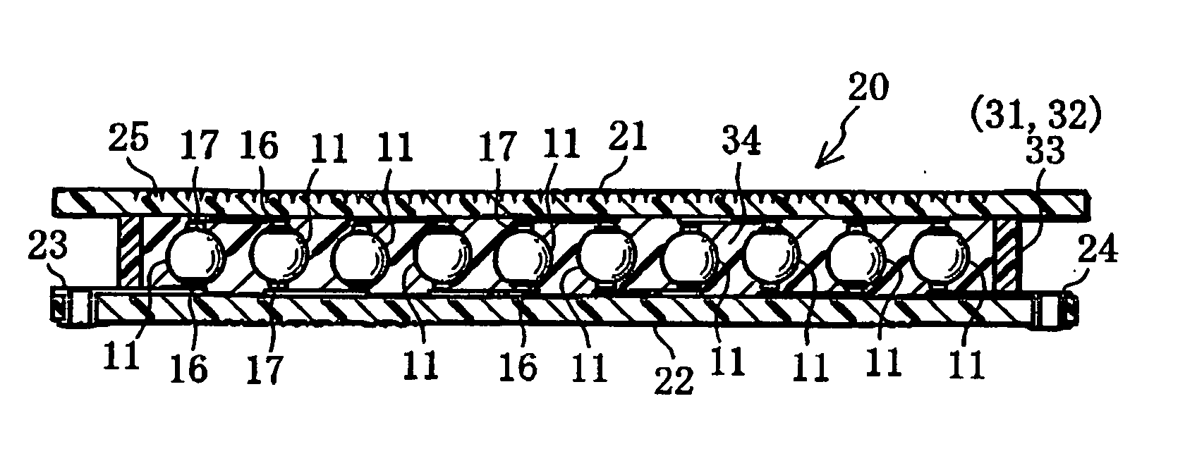
[0076] Next, a panel-form solar module can be constituted as a semiconductor module using either or both of the above two types of spherical solar cells 1 and 11. The structure of and method for manufacturing the solar module 20 employing the spherical solar cell 11 in a first embodiment will be described based on FIGS. 3 to 9.
[0077] First, the basics of the solar module 20 will be described.
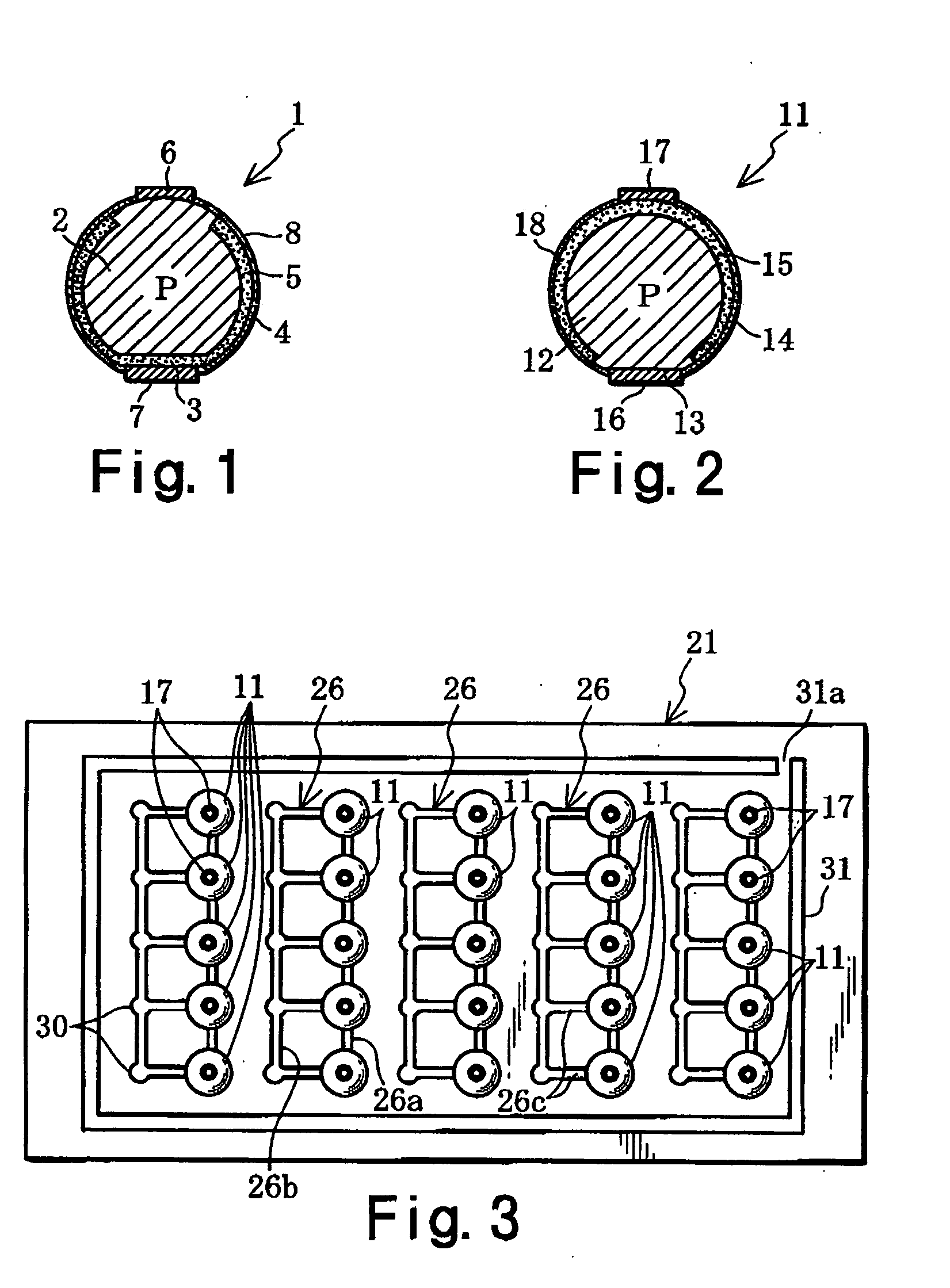
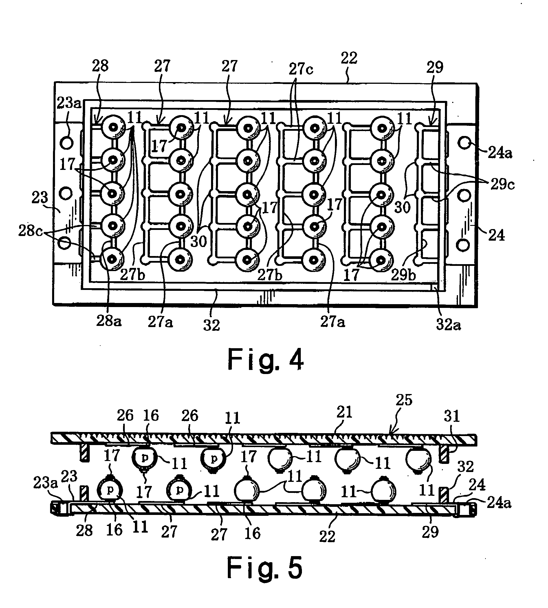
[0078] The solar module 20 is constituted such that numerous spherical solar cells 11 are incorporated in a matrix of numerous rows and columns between a pair of sheets 21, 22. If we assume that the size of this solar module 20 is 10 cm wide and 20 cm long, and the spherical solar cells 11 are laid out at a pitch of 4 mm, then the spherical solar cells 11 are disposed in a matrix of 25 rows and 50 columns, for instance. Since such a fine structure is difficult to depict, in this embodiment just a detail view will be given for the sake of facilitating understanding, using as an example a case in...
modification 1 (see figs.10 to 12)
Modification 1 (see FIGS. 10 to 12)
[0101] This solar module 40 comprises first and second sheets 41, 42, five rows and ten columns of spherical solar cells 1 and 11 incorporated in between these sheets 41, 42, a parallel connection mechanism for the parallel connection of the five spherical solar cells 1 and 11 in each column (the spherical solar cells in each group), a serial connection mechanism for the serial connection of the spherical solar cells 1 and 11 in each column with the spherical solar cells 1 and 11 in each adjacent group, and so forth. The first and second sheets 41, 42 are the same as the above-mentioned first and second sheets 21, 22. The five sets of conduction paths 46 (conductive films) formed on the inner surface of the first sheet 41 are simpler in shape than the above-mentioned conduction paths 26, but these conduction paths 46 have the same structure as the conduction paths 26, and each conduction path 46 comprises parallel connection components 46a, 46b and...
modification 2 (see figs.13 to 18)
Modification 2 (see FIGS. 13 to 18)
[0105] This solar module 60 makes use of the above-mentioned spherical solar cells 1, 11, and its structure is substantially the same as that of the solar modules 20 and 40, and it can be produced in substantially the same way, so the structure of this solar module 60 and its method of manufacture will only be described briefly.
[0106] This solar module 60 comprises first and second sheets 61, 62, six rows and 14 columns (for example) of spherical solar cells 1, 11 incorporated in between these sheets 61, 62, a parallel connection mechanism for the parallel connection of the spherical solar cells 1, 11 in each column, a serial connection mechanism for the serial connection of the spherical solar cells 1, 11 in each column with the spherical solar cells 1, 11 in each adjacent group, and so forth. The first and second sheets 61, 62 comprise sheets of transparent, reinforced water-white glass with a thickness of 3 to 4 mm, and as shown in FIG. 13, pyr...
PUM
 Abstract
Description
Claims
Application Information
 - Generate Ideas
- Intellectual Property
- Life Sciences
- Materials
- Tech Scout
- Unparalleled Data Quality
- Higher Quality Content
- 60% Fewer Hallucinations
Browse by: Latest US Patents, China's latest patents, Technical Efficacy Thesaurus, Application Domain, Technology Topic, Popular Technical Reports.
© 2025 PatSnap. All rights reserved.Legal|Privacy policy|Modern Slavery Act Transparency Statement|Sitemap|About US| Contact US: help@patsnap.com