On-chip transistor degradation monitoring

a technology of transistor degradation and monitoring, applied in the field of on-chip testing, can solve the problems of increasing the reliability problems of these transistors, increasing the problem of hot-electron effect, and increasing the degradation of transistors, so as to achieve the effect of not being burned in the integrated circui

Inactive Publication Date: 2005-06-23
INTEL CORP
View PDF4 Cites 104 Cited by
  • Summary
  • Abstract
  • Description
  • Claims
  • Application Information

AI Technical Summary

Problems solved by technology

As p-channel and n-channel field effect transistors in complementary metal oxide semiconductor integrated circuits have been scaled down, reliability problems with these transistors have increased.
In n-channel field effect transistors (NFETs) as the channel lengths have decreased, a transistor degradation sometimes referred to as a hot-electron effect has become a greater problem.
However, “burn-in” is not actually how an integra

Method used


Image

  • On-chip transistor degradation monitoring
  • On-chip transistor degradation monitoring
  • On-chip transistor degradation monitoring

Examples


Embodiment Construction

[0024] In the following detailed description of embodiments of the invention, numerous specific details are set forth in order to provide a thorough understanding of the invention. However, it will be obvious to one skilled in the art that the embodiments of the invention may be practiced without these specific details. In other instances well known methods, procedures, components, and circuits have not been described in detail so as not to unnecessarily obscure aspects of the embodiments of the invention.

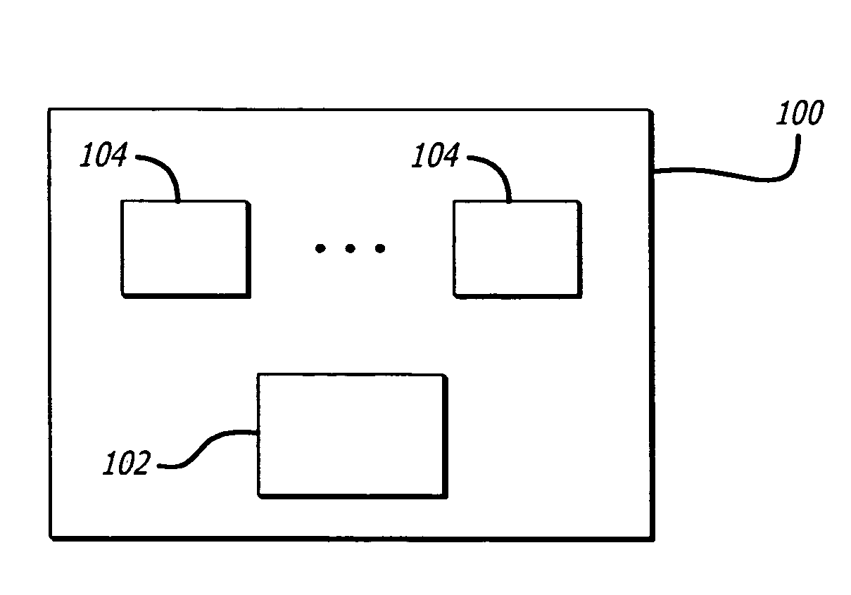
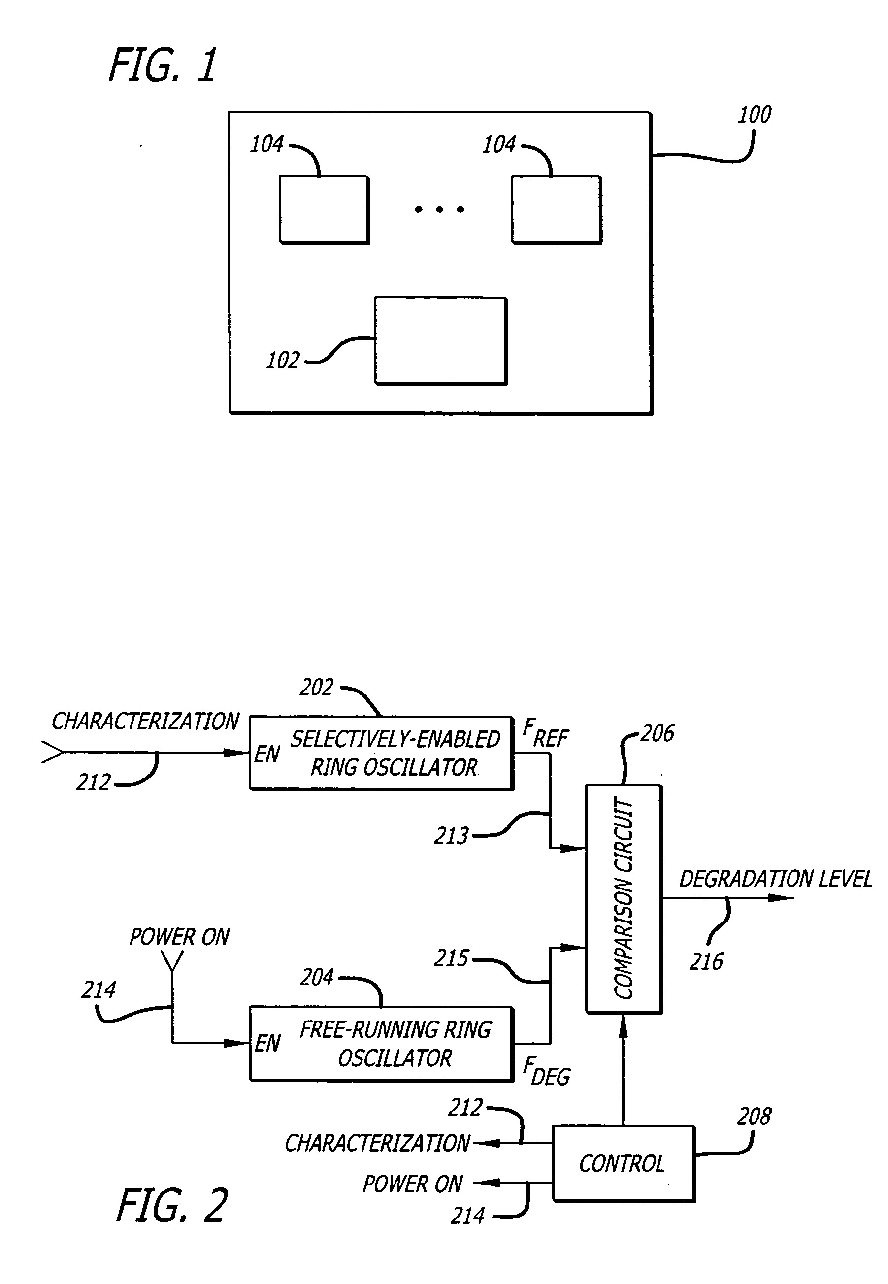
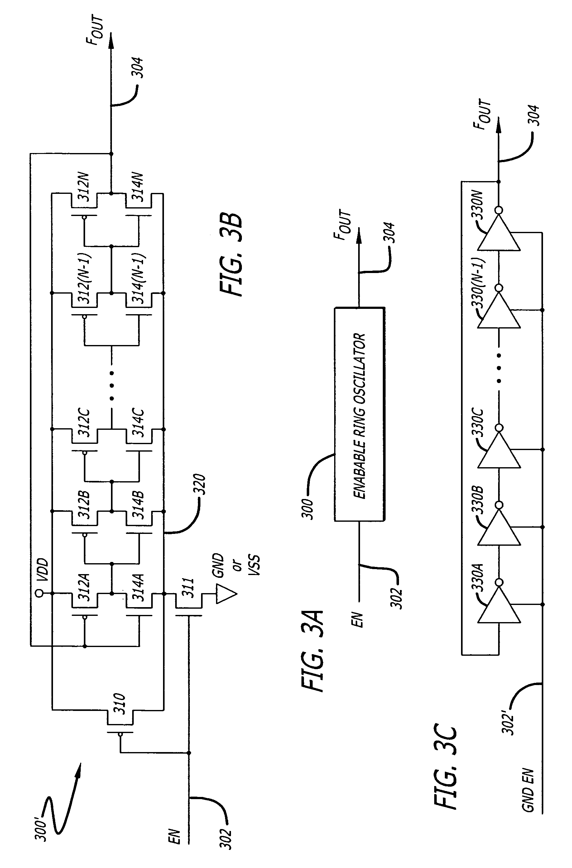
[0025] There are two known significant transistor degradation mechanisms that affect circuit performance. These significant transistor degradation mechanisms are PMOS BT transistor degradation and NMOS hot electron transistor degradation. An integrated on-chip characterization or monitoring circuit is used to quantify these two transistor degradation or aging effects. The on-chip characterization or monitoring circuit is integrated onto the same monolithic die or substrate as the ...


PUM


Abstract

Embodiments of the invention include on-chip characterization of transistor degradation. In one embodiment, includes one or more functional blocks to perform one or more functions and an integrated on-chip characterization circuit to perform on-chip characterization of transistor degradation. The integrated on-chip characterization circuit includes a selectively enabled ring oscillator to generate a reference oscillating signal, a free-running ring oscillator to generate a free-running oscillating signal, and a comparison circuit coupled to the selectively enabled ring oscillator and the free-running ring oscillator. From the reference oscillating signal and the free-running oscillating signal, the comparison circuit determine a measure of transistor degradation.

Description

FIELD OF THE INVENTION [0001] Embodiments of the invention relate generally to on-chip testing, and specifically to on-chip characterization of transistor degradation. BACKGROUND OF THE INVENTION [0002] As p-channel and n-channel field effect transistors in complementary metal oxide semiconductor integrated circuits have been scaled down, reliability problems with these transistors have increased. [0003] In n-channel field effect transistors (NFETs) as the channel lengths have decreased, a transistor degradation sometimes referred to as a hot-electron effect has become a greater problem. The hot-electron effect has been studied for quite some time now. Power supplies were accordingly reduced as the transistors were scaled down in order to minimize the hot-electron effect. Designers can design around this somewhat by increasing the channel length of a transistor or increase signal slew rates. For example the channel lengths of certain transistors that may experience greater stress, s...

Claims


Application Information

Patent Timeline
IPC IPC(8): G01R31/317
CPCG01R31/31727G01R31/31703
Inventor LIU, JONATHAN H.
Owner INTEL CORP
Why Eureka
Try Eureka