
Method for fabricating MOS field effect transistor

Inactive Publication Date: 2005-06-30
DONGBU ELECTRONICS CO LTD
View PDF1 Cites 1 Cited by
  • Summary
  • Abstract
  • Description
  • Claims
  • Application Information

AI Technical Summary

Benefits of technology

[0013] To address the above-described and other problems, it is an object of the present invention to provide a method of fabricating a MOS field effect transistor. A gate insulating film and a gate conductive film are formed on a semiconductor substrate. The gate conductive film is patterned to form a first gate conductive film having a thin thickness and a second gate conductive film having a thick thickness. An insulating film pattern is formed on a side wall of the second gat

Problems solved by technology

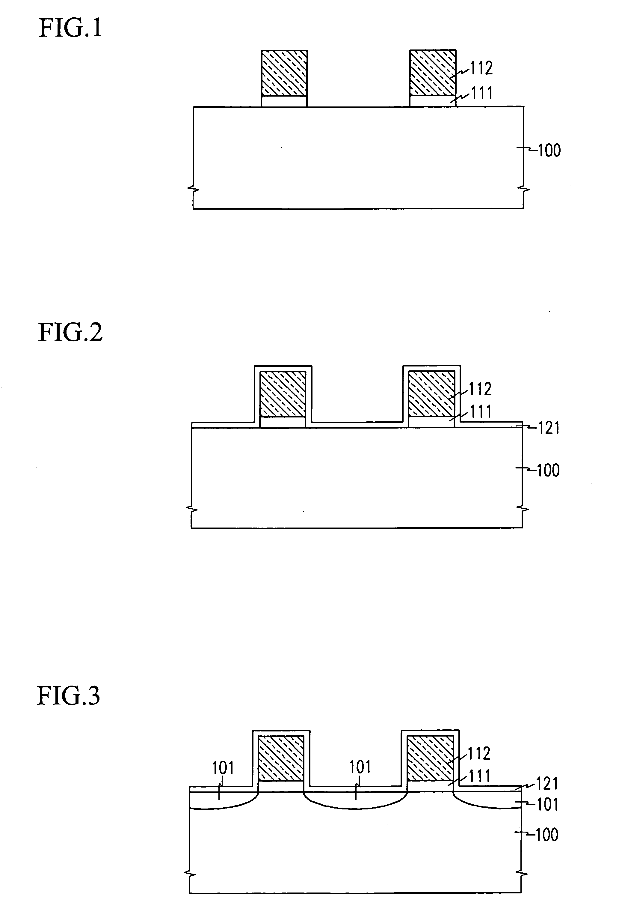
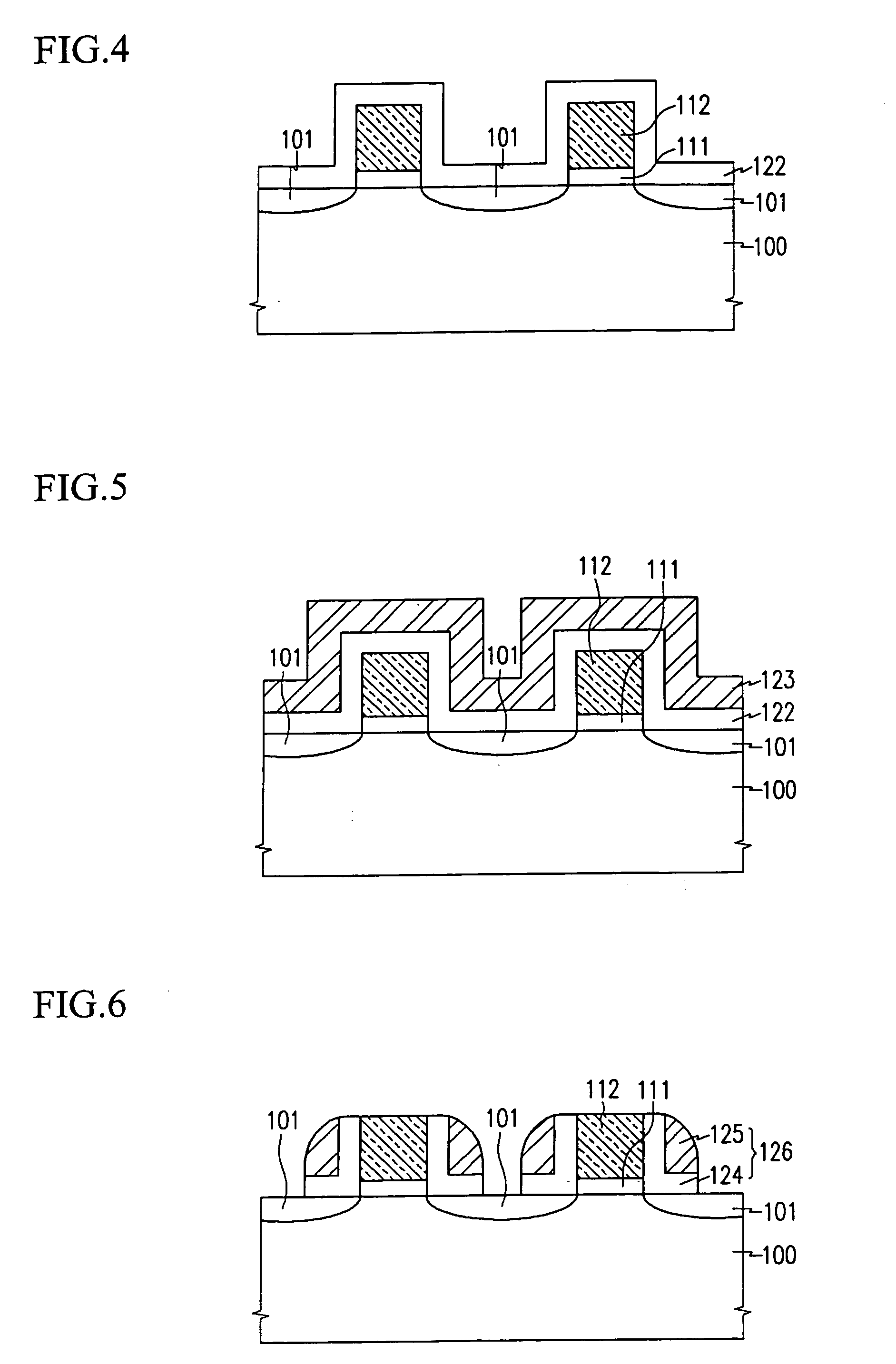
As a result, when the interlayer insulating film is formed, the gap between the adjacent gate conductive film patterns 112 may not be completely filled with the interlayer insulating film, such that voids are generated.
The voids act as cracks and bridges deteriorating reliability of the device through subsequent thermal and contact processes.
For example, in a SRAM, which has a low operation voltage and in which leakage current characteristics are critical, a silicide process may not be performed.

Method used


Image

  • Method for fabricating MOS field effect transistor
  • Method for fabricating MOS field effect transistor
  • Method for fabricating MOS field effect transistor

Examples


Embodiment Construction

[0018] Embodiments of the present invention are described with reference to the accompanying drawings. It is to be understood that the invention is not limited to the disclosed embodiments, but rather is intended to cover various modifications and arrangements within the scope of the claims.

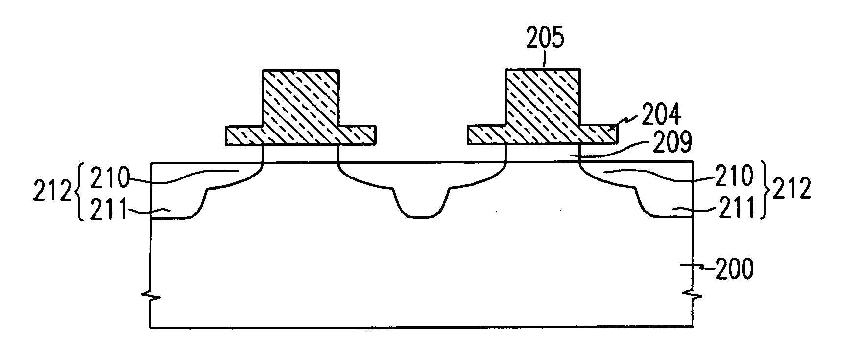
[0019]FIGS. 8-14 are sectional views illustrating a method of fabricating a MOS field effect transistor according to the present invention.

[0020] As shown in FIG. 8, a gate insulating film 201 and a gate conductive film 202 are formed on a semiconductor substrate 200. Preferably, the films 201 and 202 are sequentially formed. In a preferred embodiment, the gate insulating film 201 is formed from an oxide film and the gate conductive film 202 is formed from a polysilicon film.

[0021] A mask pattern 203, which is used to pattern the gate conductive film 202, is formed on the gate conductive film 202. The mask pattern 203 acts as a photoresist pattern.

[0022] As shown in FIG. 9, an exposed portion...


PUM


Abstract

A method of fabricating a MOS field effect transistor. A gate insulating film and a gate conductive film are formed on a semiconductor substrate. The gate conductive film is patterned to form a first gate conductive film having a thin thickness and a second gate conductive film having a thick thickness. An insulating film pattern is formed on a side wall of the second gate conductive film. The insulating film pattern is used as an etching mask to remove exposed portions of the first gate conductive film and the gate insulating film. An etch process is performed to remove the insulating film pattern and a portion of the gate insulating film under the first gate conductive film. An ion implantation process is performed using the first gate conductive film as an ion implantation buffer for a lightly doped impurity region to form a source / drain region.

Description

BACKGROUND OF THE INVENTION [0001] (a) Field of the Invention [0002] The present invention relates to a method of fabricating a semiconductor device, and more particularly to a method of fabricating a MOS field effect transistor. [0003] (b) Discussion of the Related Art [0004] Known semiconductor devices have a single source / drain junction structure. Recently, as semiconductor devices become increasingly integrated, channel lengths decrease. A source / drain region having a lightly doped drain (LDD) junction structure is used to reduce undesirable effects caused by decreased channel lengths. [0005]FIGS. 1-7 are sectional views illustrating a method of fabricating a related art MOS field effect transistor. As shown in FIG. 1, a gate insulating film pattern 111 and a gate conductive film pattern 112 are stacked sequentially on a semiconductor substrate 100. It is known to form a typical device isolation field and a well region before the gate insulating film pattern 111 and the gate con...

Claims


Application Information

Patent Timeline
IPC IPC(8): H01L21/28H01L21/336H01L21/8234H01L29/78
CPCH01L21/28114H01L21/823425H01L29/66598H01L21/823468H01L21/823456H01L21/18
Inventor KIM, DAE-KYEUN
Owner DONGBU ELECTRONICS CO LTD
Learn More