Light emitting device and production system of the same

a technology of light emitting devices and production systems, applied in the field of electroluminescent panels, can solve the problems of not being able to provide realistically a power source for supplying voltage, and putting light emitting devices into practical use, and achieve the effect of reducing luminance and limiting non-uniform luminan

Inactive Publication Date: 2005-07-21
SEMICON ENERGY LAB CO LTD
View PDF43 Cites 254 Cited by
  • Summary
  • Abstract
  • Description
  • Claims
  • Application Information

AI Technical Summary

Benefits of technology

[0021] It is a purpose of the invention in view of the over-described to provide a light emitting device capable of restraining nonuniformity of luminance caused by a deterioration in an field light emitting layer or a dispersion in a TFT characteristic among pixels and capable of restraining a reduction in the luminance of a total of a screen and a production system of the light emitting device.

Problems solved by technology

Meanwhile, lowering of luminance of OLED in accordance with a deterioration in an electroluminescent material poses a serious problem in putting light emitting devices into practical use.
However, it is not realistic to provide a power source for supplying voltage or current in correspondence with each pixel and therefore, actually, a common power source for supply voltage or current for-all of pixels or a certain number of pixel is provided.

Method used


Image

  • Light emitting device and production system of the same
  • Light emitting device and production system of the same
  • Light emitting device and production system of the same

Examples


embodiment 1

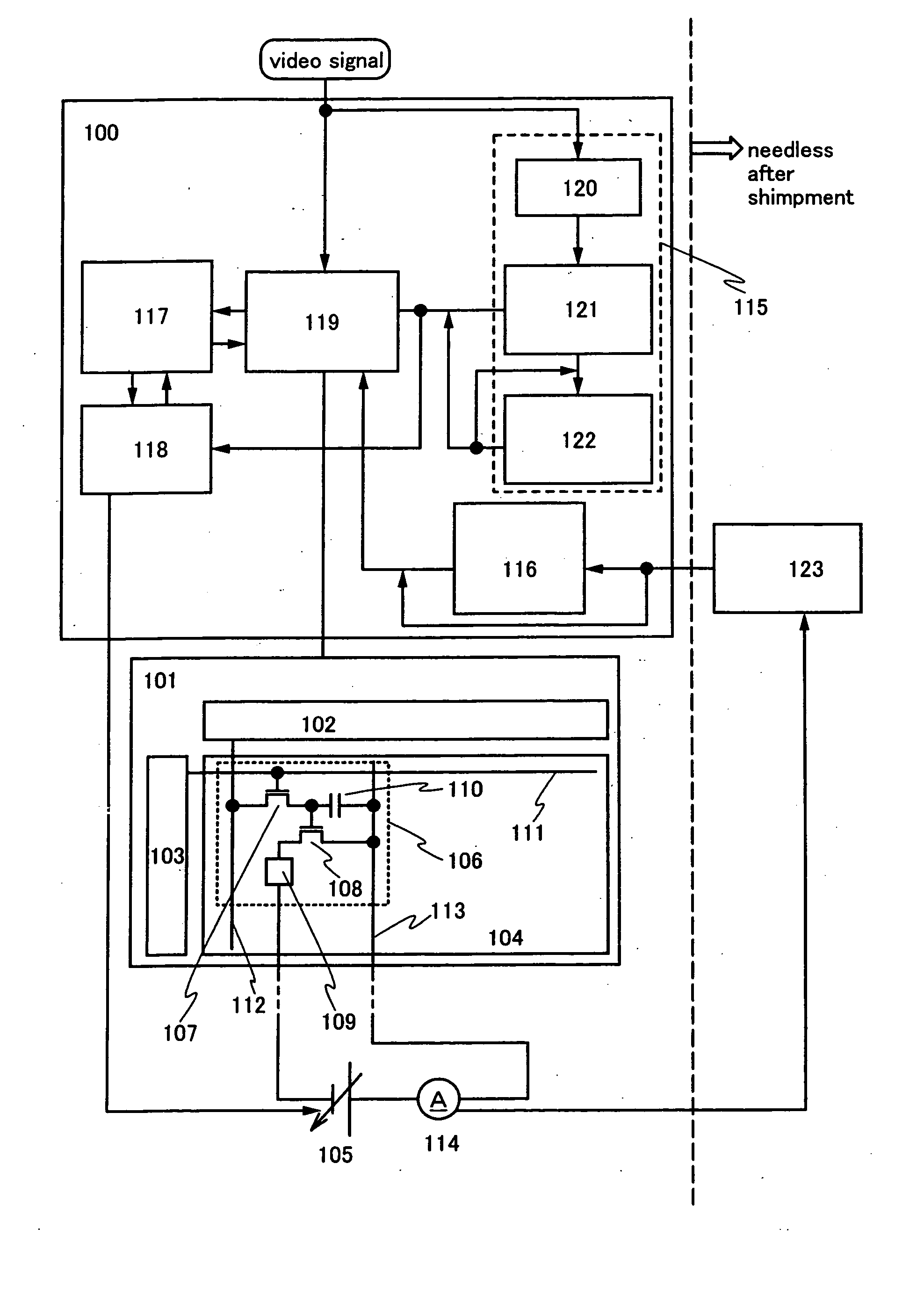
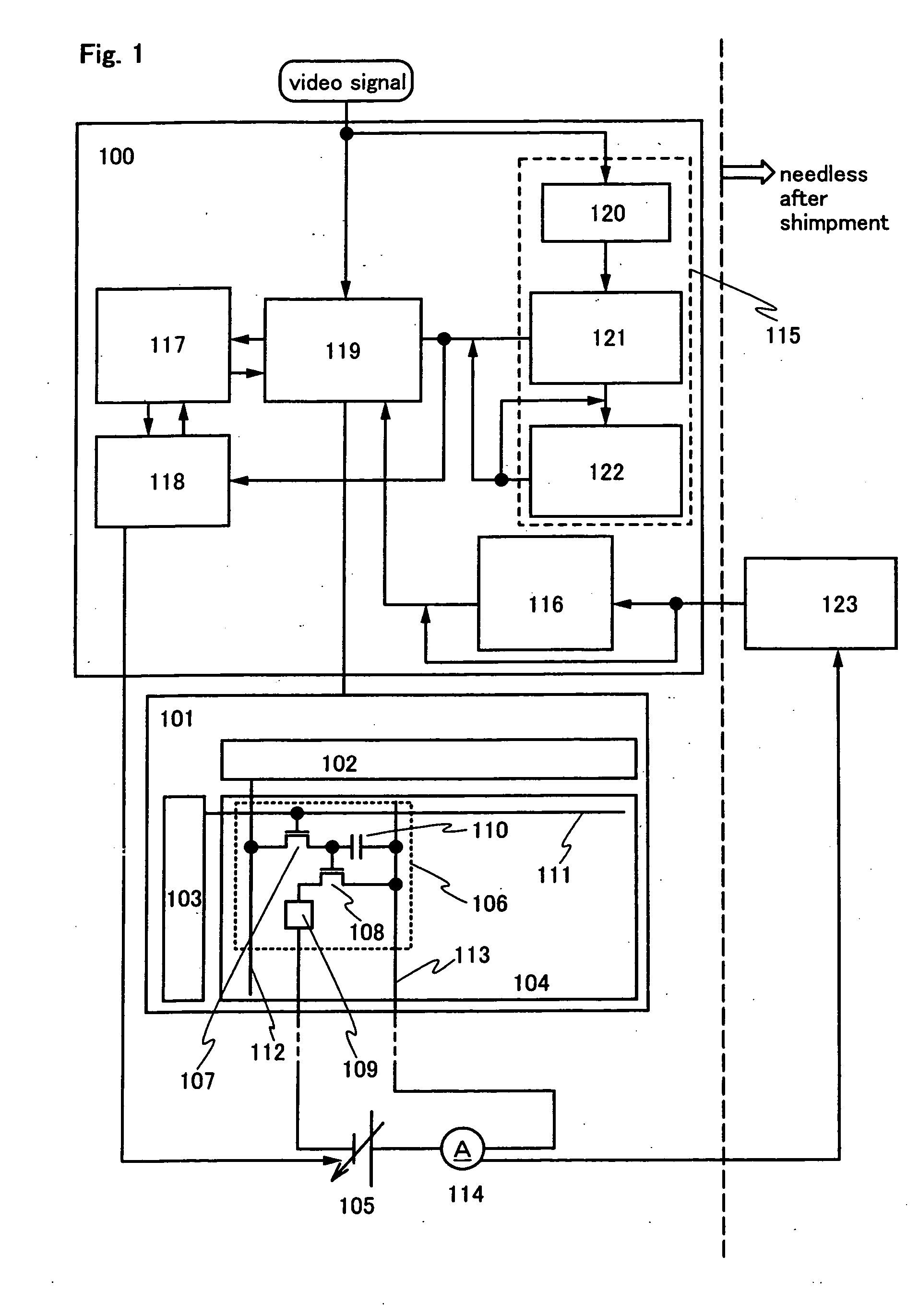
[0056] A constitution of a light emitting device of the invention will be explained as follows. FIG. 1 is a block diagram of a light emitting device of the invention including a correcting circuit 100, a panel 101 and a voltage source 105. Further, other than these, a circuit necessary for driving a controller or the like may be included.

[0057] The panel 101 shown in FIG. 1 includes a signal line drive circuit 102, a scanning line drive circuit 103 and a pixel portion 104. Further, although in FIG. 1, the correcting circuit 100 and the voltage source 105 are formed over a substrate different from an element substrate formed with the signal line drive circuit 102, the scanning line drive circuit 103 and the pixel portion 104, these may be formed over the same substrate when possible. Further, the signal line drive circuit 102 and the scanning line drive circuit 103 may be formed over a substrate different from the element substrate formed with the pixel portion 104. Although connect...

embodiment 2

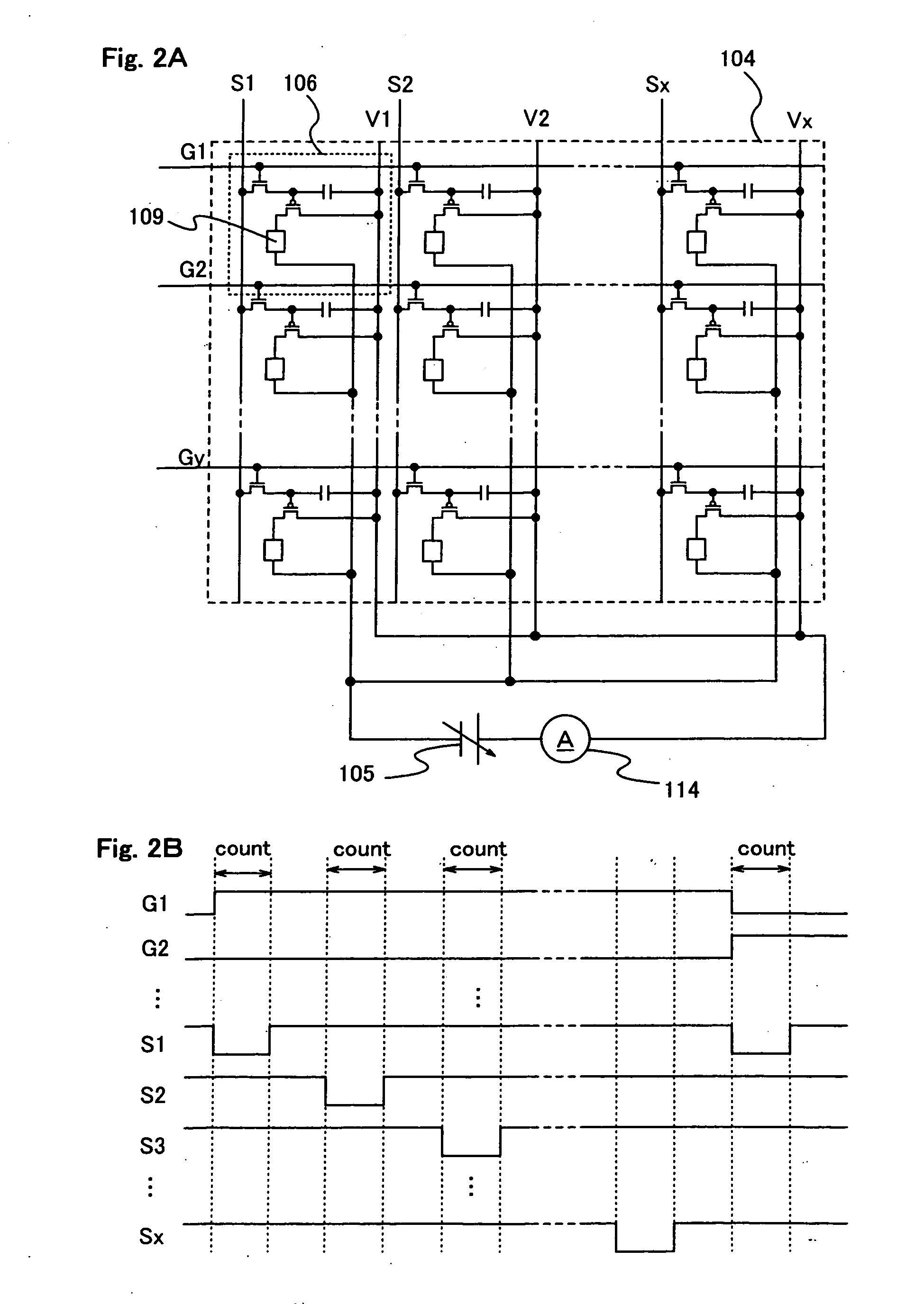
[0103] According to Embodiment 1, an explanation has been given with regard to an example of grasping the dispersion of the characteristics of the driving TFTs by using data of the current amount of each pixel and making the gray scales of pixels uniform. The current flowing in the light emitting element and the luminance are in a proportional relationship and therefore, the dispersion of the luminance of the light emitting element may be regarded as the dispersion of flowing current. Therefore, the gray scale of each pixel can also be corrected by using data of the luminance of each pixel instead of data of the current amount of each pixel. According to the embodiment, an explanation will be given with regard to an example of making the gray scale of pixels uniform by using data of the luminance of pixels instead of data of the current amount of each pixel.

[0104] There are various methods of measuring the luminance of the light emitting element. FIG. 19A shows an example of measur...

embodiment 3

[0116] In embodiment 1, both the voltage correcting circuit 118 and the video signal correcting circuit 119 compare data of the change over time of the luminance, data of the change of the luminance relative to the current amount, or the like, which are previously stored to the deterioration characteristic correcting data storing portion 117 with data obtained by accumulating the information with regard to the number of gray scale of each pixel stored to the nonvolatile memory for video signal 122 and grasp a degree of deterioration of each pixel.

[0117] An explanation with regard to a structure different from Embodiment 1 will be given in this Embodiment. In this Embodiment, in the video signal correcting circuit 119, video signals are corrected by the data with regard to the degree of deterioration of each pixel obtained in the voltage correcting circuit 118.

[0118] By the above structure, in the video signal correcting circuit 119, it is omitted to compare data of the change over...


PUM


Abstract

To provide a light emitting device without nonuniformity of luminance, a correcting circuit for correcting a video signal supplied to each pixel to a light emitting device. The correcting circuit is stored with data of a dispersion of a characteristic of a driving TFT among pixels and data of a change over time of luminance of a light emitting element. Further, by correcting a video signal inputted to the light emitting device in conformity with a characteristic of the driving TFT of each pixel and a degree of a deterioration of the light emitting element based on the over-described two data, nonuniformity of luminance caused by a deterioration of an electroluminescent layer and nonuniformity of luminance caused by dispersion of a characteristic of the driving TFT are restrained.

Description

BACKGROUND OF THE INVENTION [0001] 1. Field of the Invention [0002] The present invention relates to an electroluminescent panel (hereinafter, simply referred to as panel) sealing a light emitting element formed over a substrate between the substrate and a cover member. Further, the invention relates to an electroluminescent module where an IC including a controller is mounted over the panel. Further, in the specification, both of the panel and the electroluminescent module are generally referred to as luminescent device. [0003] 2. Description of the Related Art [0004] A light emitting element spontaneously emits light and therefore, having high visibility, dispensing with a backlight needed in a liquid crystal display display (LCD), optimum for thin formation and not restricted in viewing angle. Therefore, in recent years, a luminescent device using a light emitting element attract attention as a display device substituting for CRT or LCD. [0005] Further, in the specification, a li...

Claims


Application Information

Patent Timeline
Patent Type & Authority Applications(United States)
IPC IPC(8): G09G3/00G09G3/20G09G3/32
CPCG09G3/006G09G2320/0693G09G3/3233G09G3/3266G09G3/3291G09G2300/0809G09G2300/0842G09G2300/0852G09G2300/0861G09G2310/061G09G2320/0233G09G2320/0285G09G2320/029G09G2320/0295G09G2320/043G09G2320/048G09G3/2022
Inventor YAMAZAKI, SHUNPEIKIMURA, HAJIMEAKIBA, MAIANZAI, AYAYAMAZAKI, YU
Owner SEMICON ENERGY LAB CO LTD
Why Eureka
Try Eureka