Probe with trapezoidal contactor and device based on application thereof, and method of producing them

Inactive Publication Date: 2005-07-28
TOKYO ELECTRON LTD
View PDF9 Cites 21 Cited by
  • Summary
  • Abstract
  • Description
  • Claims
  • Application Information

AI Technical Summary

Benefits of technology

[0009] In accordance with still another aspect of the present invention, it is still another object of the present invention to provide a probe attaching method and a probe attac

Problems solved by technology

Accordingly, the required number of the photomasks increases greatly such that lots of time and cost are n

Method used


Image

  • Probe with trapezoidal contactor and device based on application thereof, and method of producing them
  • Probe with trapezoidal contactor and device based on application thereof, and method of producing them
  • Probe with trapezoidal contactor and device based on application thereof, and method of producing them

Examples


first embodiment

[0080] Hereinafter, the present invention is described in accordance with a first embodiment with reference to FIGS. 1 to 8E.

[0081] A probe in accordance with the present invention is not only used to be attached to a probe card, but also may be adopted for various usages such as a probe to be attached as a terminal for diverse measurement devices, a terminal of an electronics circuit, and the like. Herein, from an aspect of explaining the probe of the present invention more concretely, the probe attached to the probe card will be described. However, the probe in accordance with the present invention is not limited to a usage for being attached to the probe card. An embodiment of the probe card to which the probe of the present invention is attached will now be described with reference to FIGS. 1 to 3.

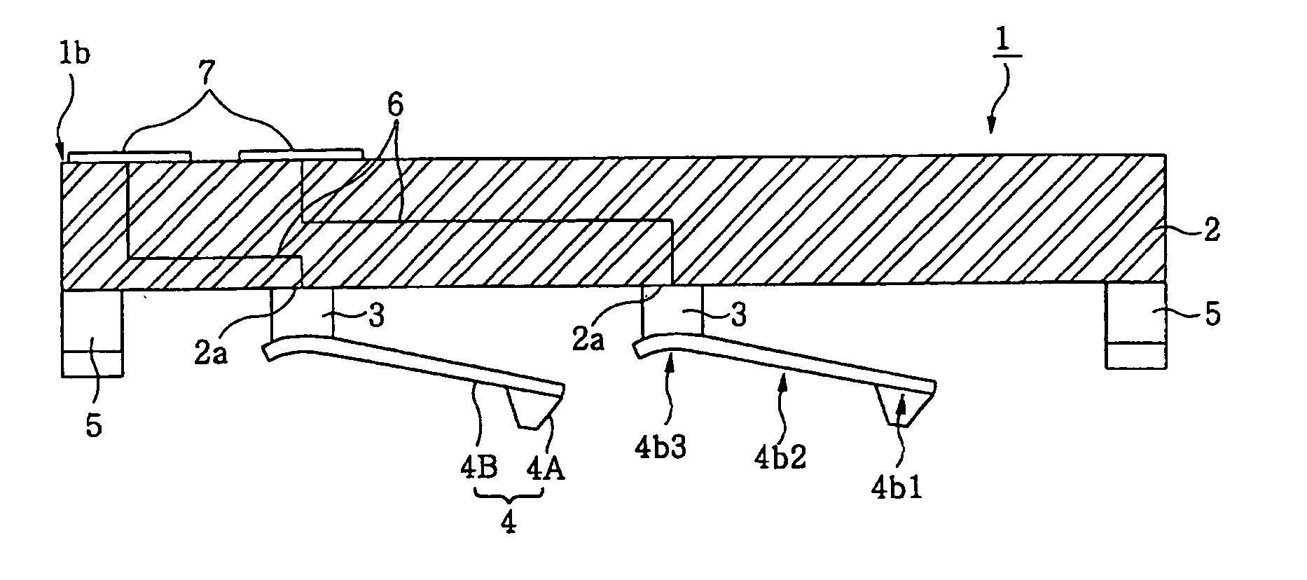
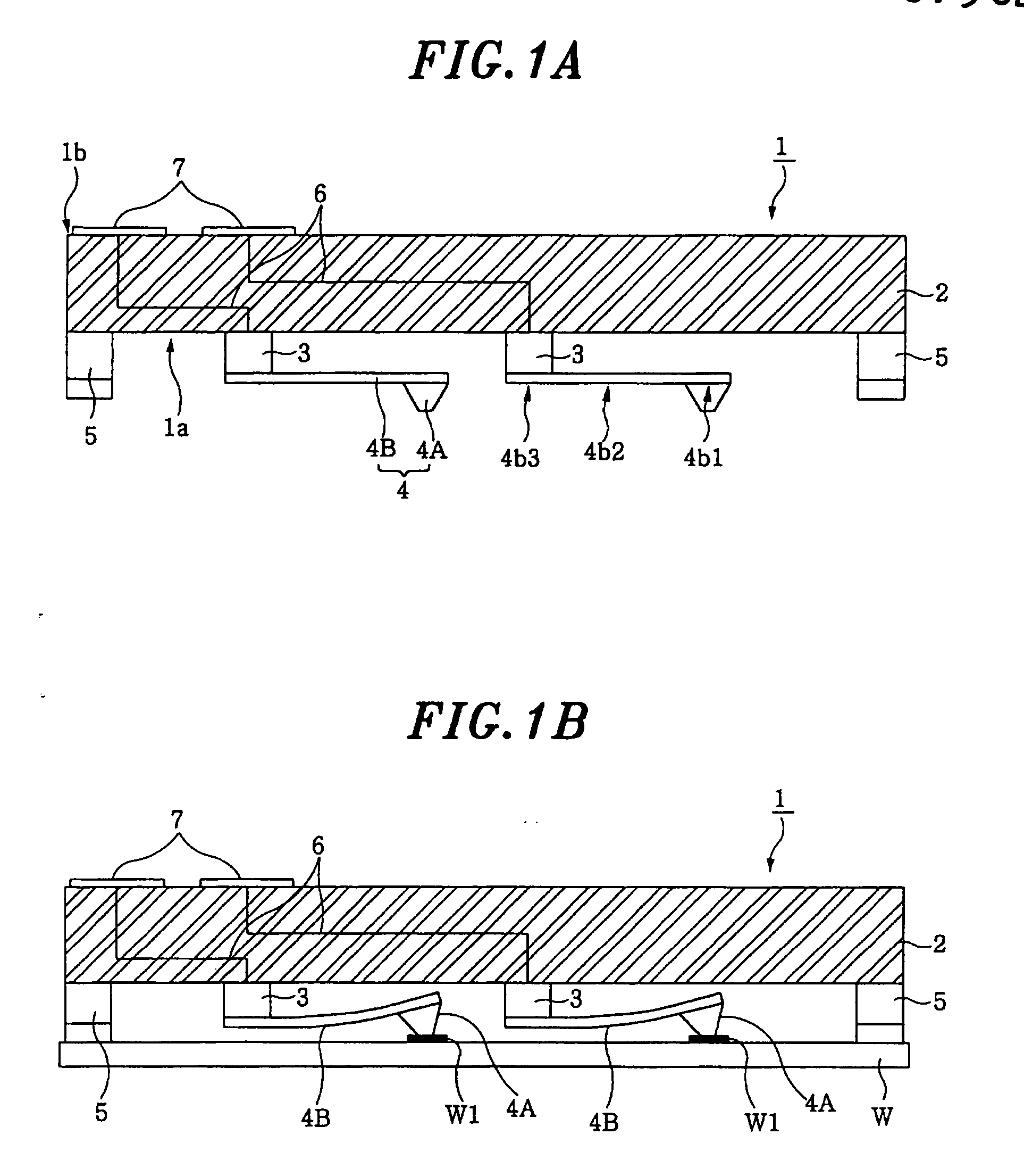
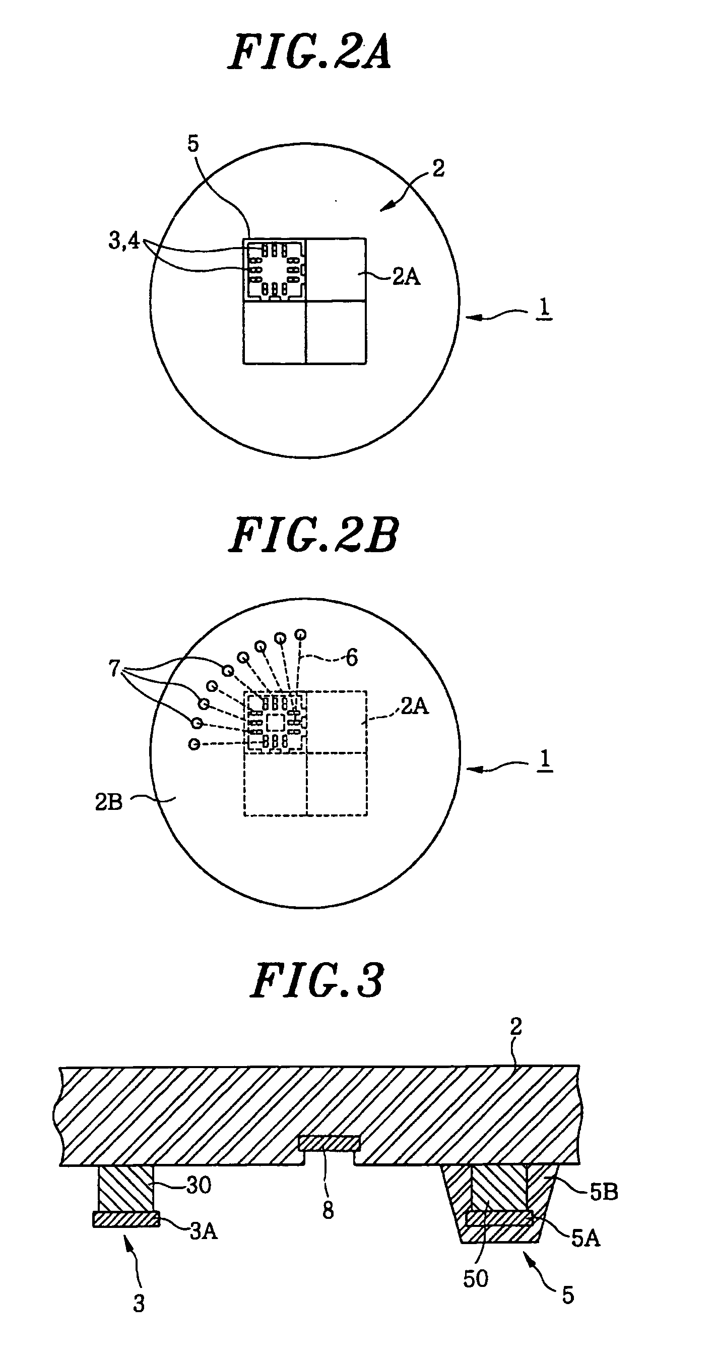
[0082] As shown in FIGS. 1A, 1B and FIGS. 2A, 2B, the probe card 1 includes a card shaped substrate (hereinafter, referred to as a probe card main body) 2, and the probe card main bod...

second embodiment

[0167] In accordance with the first and the present invention, there are provided a probe and a method thereof for mass producing the probe used commonly to the various probe cards, each of which having a different array pattern.

[0168] In accordance with the first and the second embodiment of the present invention, a small quantity of many kinds of the probe cards are manufactured economically without a photomask to manufacture the original probe.

[0169] There are provided a probe attaching method and an apparatus thereof for manufacturing various probe cards at a low cost, by using one kind of the probe.

[0170] In accordance with the present invention, it is provided a probe card manufactured by attaching one kind of the probe based on the array thereof.


PUM

PropertyMeasurementUnit
Currentaaaaaaaaaa
Currentaaaaaaaaaa
Currentaaaaaaaaaa

Abstract

A probe is disclosed, comprising a beam 4B, which has a front end 4b1, an intermediate portion 4b2 and a base end 4b3, the front end being a portion for contacting a test subject through a contactor, the base end being a portion for fixing the probe; and a substantially trapezoidal contactor 4A, which is fixed to the leading end 4b1 of the beam.

Description

FIELD OF THE INVENTION [0001] The present invention relates to a probe used for inspecting electrical characteristics of semiconductor devices having a shape of, e.g., a semiconductor wafer, a method for manufacturing the probe, a probe array, a method for manufacturing the probe array, a method for attaching the probe, an apparatus for attaching the probe, a probe card and a probe array maintenance unit. BACKGROUND OF THE INVENTION [0002] A probe card is used to inspect electrical characteristics of a test subject, for example, a semiconductor device (IC chip) such as a memory circuit or a logic circuit, formed on a semiconductor wafer (hereinafter, referred to as a wafer for simplicity) in large numbers. The probe card includes a plurality of probes, each of the probes being installed to be correspondent to a plurality of electrode pads formed on the test subject (for example, IC chip). Each probe makes an electrical connection between a tester and the IC chip by contacting electr...

Claims


Application Information

Patent Timeline
IPC IPC(8): G01R1/067G01R31/26G01R1/073G01R3/00H01L21/66
CPCG01R1/06738G01R1/06744G01R1/06755G01R1/07342G01R1/0735G01R3/00Y10T29/49155Y10T29/49222Y10T29/49218Y10T29/49213Y10T29/49204Y10T29/49208G01R1/06727H01L22/00
Inventor HOSAKA, HISATOMITAKEKOSHI, KIYOSHI
Owner TOKYO ELECTRON LTD
Why Eureka
Try Eureka