
Multi-layer printed circuit board and method for manufacturing the same

Active Publication Date: 2005-08-25
MURATA MFG CO LTD
View PDF8 Cites 7 Cited by
  • Summary
  • Abstract
  • Description
  • Claims
  • Application Information

AI Technical Summary

Benefits of technology

[0009] In view of the above-described problem, it is an object of the present invention to provide a multi-layer printed circuit board and a method for manufacturing the same. The manufacturing cost of the multi-layer printed circuit board is small, and a conductive pattern of the multi-layer printed circuit board is prevented from peeling off. Further, the multi-layer printed circuit board is suitable for providing a high frequency circuit.
[0011] In the multi-layer printed circuit board, the surface roughness of the surface conductive pattern on the insulation substrate side is set to be large in order to increase adhesive strength so that the surface conductive pattern exposed on the surface of the multi-layer printed circuit board does not peel off easily. On the other hand, although the surface roughness of the inner conductive pattern is smaller than that of the surface conductive pattern on the insulation substrate side, an external force for peeling off the inner conductive pattern does not apply to the inner conductive pattern. That is because the inner conductive pattern is embedded in the multi-layer printed circuit board. Thus, the multi-layer printed circuit board has the surface and inner conductive patterns prevented from peeling off.
[0012] Preferably, the inner conductive pattern includes a high frequency conductive pattern for providing a high frequency circuit. In this case, the surface roughness of the inner conductive pattern is set to be smaller than that of the surface conductive pattern on the insulation substrate side. Therefore, the surface resistance of the inner conductive pattern is smaller than that of the surface conductive pattern, so that the inner conductive pattern has excellent properties as a conductive wire for flowing a high frequency alternating current, which is superior to the surface conductive pattern. Accordingly, the multi-layer printed circuit board having the inner conductive pattern used as the high frequency conductive pattern is suitable for providing the high frequency circuit.
[0016] The method provides to manufacture the multi-layer printed circuit board having the conductive patterns disposed on the surface of the circuit board and / or disposed inside of the circuit board. The conductive patterns are prevented from peeling off. Further, when the inner conductive pattern of the multi-layer printed circuit board is used for the high frequency conductive pattern, the multi-layer printed circuit board is suitable for providing the high frequency circuit.
[0018] The method provides to manufacture the multi-layer printed circuit board having the conductive patterns disposed on the surface of the circuit board and / or disposed inside of the circuit board. The conductive patterns are prevented from peeling off. Further, when the inner conductive pattern of the multi-layer printed circuit board is used for the high frequency conductive pattern, the multi-layer printed circuit board is suitable for providing the high frequency circuit.

Problems solved by technology

However, not only the dielectric constant of the insulation layer but also the surface roughness of the wiring layer affect the high frequency properties of the signal.
Therefore, the properties of a high frequency alternating current flowing through the wiring layer are deteriorated.
Thus, the surface roughness of the wiring layer affects the high frequency properties largely.
Thus, the manufacturing cost becomes small.
However, when the surface roughness of the conductive pattern becomes small in order to improve the high frequency properties, the conductive pattern exposed on the surface of the multi-layer printed circuit board easily peels off.

Method used


Image

  • Multi-layer printed circuit board and method for manufacturing the same
  • Multi-layer printed circuit board and method for manufacturing the same
  • Multi-layer printed circuit board and method for manufacturing the same

Examples


Embodiment Construction

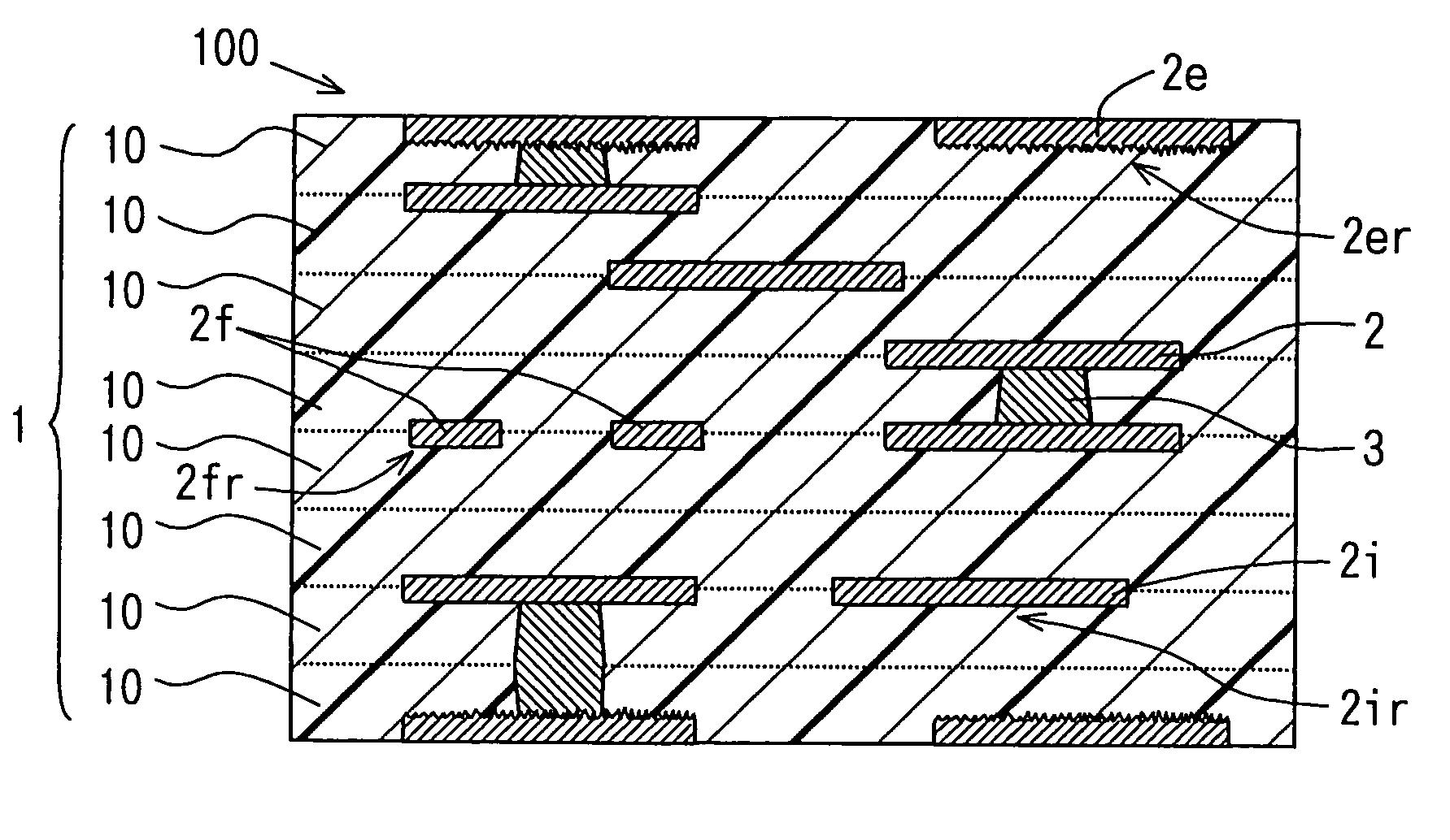
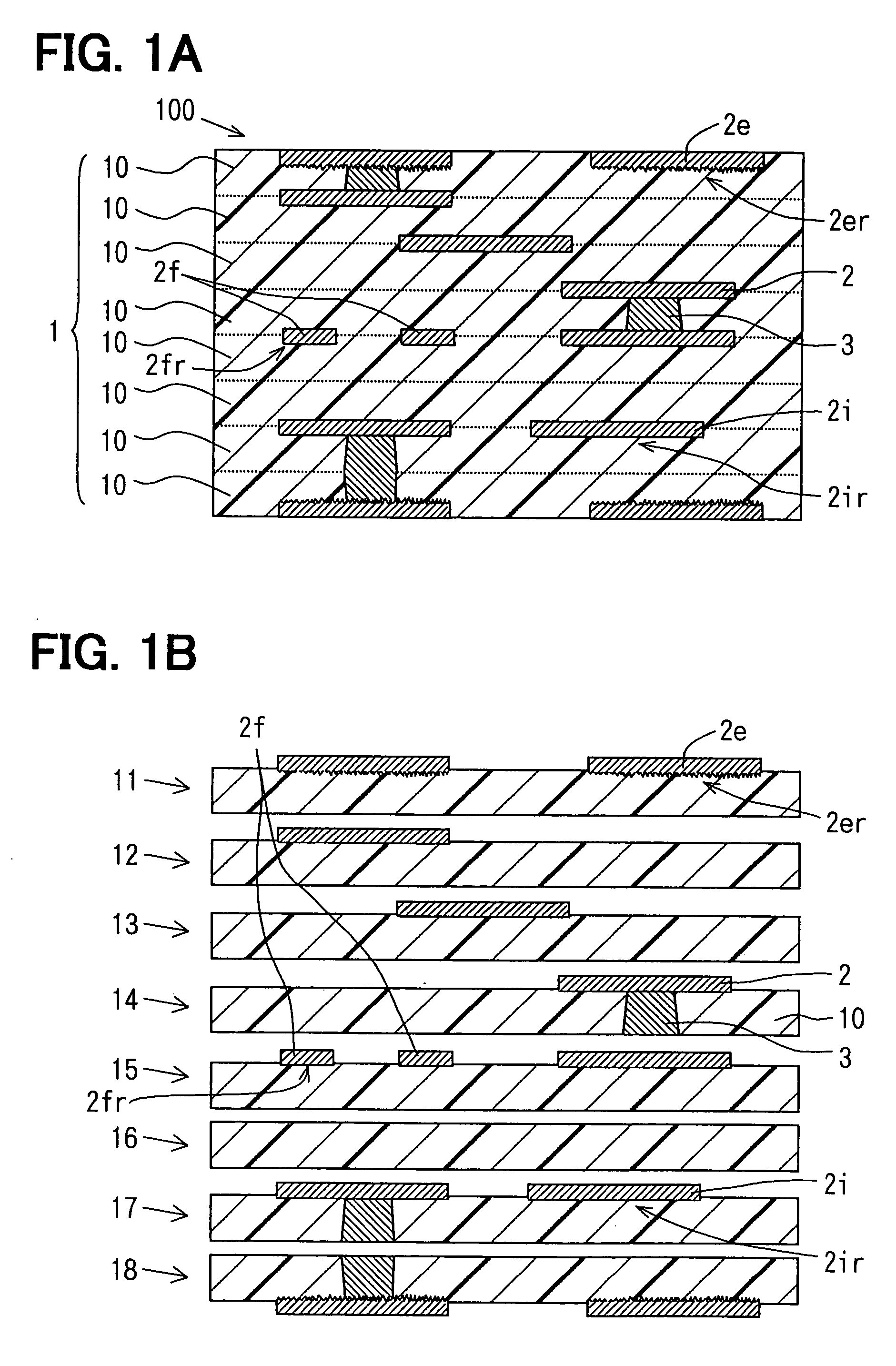
[0024] A multi-layer printed circuit board 100 according to a preferred embodiment of the present invention is shown in FIG. 1A. FIG. 1B explains a laminating state of each constituent element in process of manufacturing the multi-layer printed circuit board 100.

[0025] The multi-layer printed circuit board 100 shown in FIG. 1A includes an insulation substrate 1 made of thermoplastic resin and a wiring layer for providing a conductive pattern 2 made of metallic film. Specifically, the multi-layer printed circuit board 100 includes, for example, eight conductive pattern films 11-18 laminated and bonded together, as shown in FIG. 1B. Each conductive pattern film 11-18 includes a resin film 10 made of thermoplastic resin and the conductive pattern 2. The conductive pattern 2 made of metallic film has a predetermined pattern, and is disposed on the resin film 10. The thermoplastic resin for providing the insulation substrate 1 shown in FIG. 1A and the resin film 10 composing the insulat...


PUM

PropertyMeasurementUnit
Electrical conductoraaaaaaaaaa
Surface roughnessaaaaaaaaaa

Abstract

A multi-layer printed circuit board includes an insulation substrate; a surface conductive pattern disposed on a surface of the insulation substrate; and an inner conductive pattern embedded in the insulation substrate. The surface conductive pattern has a surface roughness on an insulation substrate side, the surface roughness of the surface conductive pattern being larger than that of the inner conductive pattern.

Description

CROSS REFERENCE TO RELATED APPLICATION [0001] This application is based on Japanese Patent Application No. 2003-101460 filed on Apr. 4, 2003, the disclosure of which is incorporated herein by reference. FIELD OF THE INVENTION [0002] The present invention relates to a multi-layer printed circuit board and a method for manufacturing the same. The multi-layer printed circuit board includes an insulation layer and a wiring layer formed of a conductive pattern, which are laminated alternately. Specifically, the present invention relates to a multi-layer printed circuit board suitably used for a high frequency circuit and a method for manufacturing the same. BACKGROUND OF THE INVENTION [0003] A multi-layer printed circuit board used for a high frequency circuit is, for example, disclosed in Japanese Patent Application Publication No. H01-120095 (i.e., U.S. Pat. No. 4,931,354). The multi-layer printed circuit board includes multiple insulation layers made of ceramics and multiple wiring la...

Claims


Application Information

Patent Timeline
IPC IPC(8): H05K1/02H05K3/38H05K1/11H05K3/46
CPCH05K1/024H05K1/0242H05K3/382H05K3/4617H05K3/4632H05K2201/0129Y10T29/49126H05K2201/0352H05K2203/065Y10T29/49128Y10T428/24917Y10T29/49155Y10T29/49163H05K2201/0191F24F6/02F24F2006/006
Inventor HARADA, TOSHIKAZUKONDO, KOJI
Owner MURATA MFG CO LTD
Learn More