

Micro electronic component
a technology of electronic components and components, applied in the field of micro electronic components, can solve problems such as defective connections, and achieve the effect of simple bonding and simple design
- Summary
- Abstract
- Description
- Claims
- Application Information
AI Technical Summary
Benefits of technology
Problems solved by technology
Method used
Image

Examples
Embodiment Construction
[0019] For the purposes of promoting an understanding of the principles of the invention, reference will now be made to the embodiments illustrated in the drawings and specific language will be used to describe the same. It will nevertheless be understood that no limitation of the scope of the invention is thereby intended, such alterations and further modifications in the illustrated device, and such further applications of the principles of the invention as illustrated therein being contemplated as would normally occur to one skilled in the art to which the invention relates.
[0020] Referring to FIGS. 1-4, it should first be noted that, in the figures, the same reference symbols are used for equivalent or similar parts, wherein corresponding or comparable properties and advantages are achieved even if a description is not repeated, especially due to reasons of simplification.
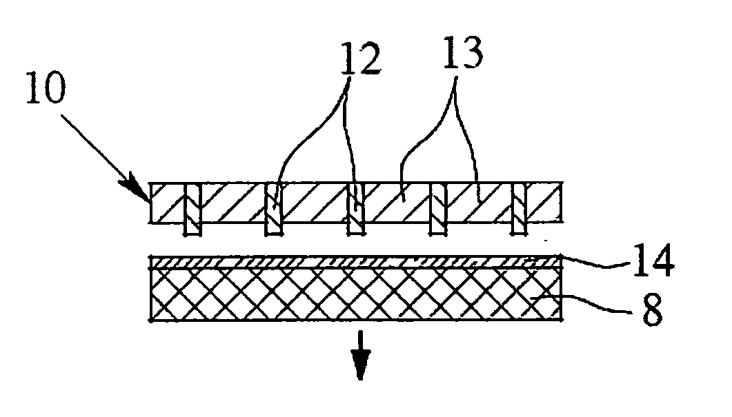
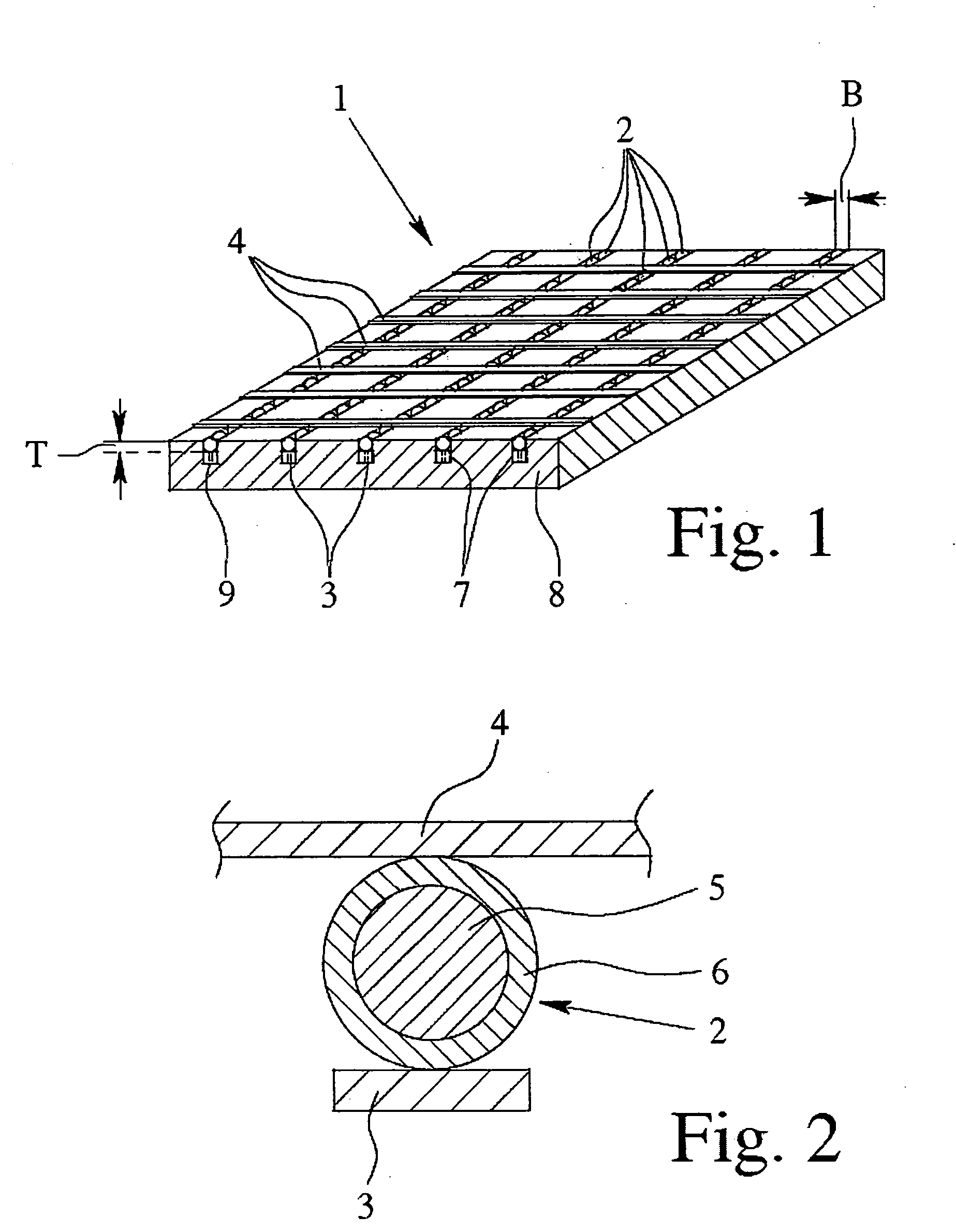
[0021]FIG. 1 shows in a schematic, perspective illustration a micro electronic component 1 according to an...
PUM
 Abstract
Description
Claims
Application Information