Semiconductor storage device

a storage device and semiconductor technology, applied in the field of semiconductor storage devices, can solve the problems of reducing the busy rate of refresh compared with the conventional dram, affecting and affecting the fabrication of semiconductor devices, so as to achieve the effect of not lowering the performance of read/write operations

Inactive Publication Date: 2005-10-20
KK TOSHIBA
View PDF15 Cites 111 Cited by
  • Summary
  • Abstract
  • Description
  • Claims
  • Application Information

AI Technical Summary

Benefits of technology

[0008] An object of the present invention is to provide a semiconductor storage device that does not lower the performance of the read / write operation for the FBC.

Problems solved by technology

As for a conventional DRAM cell including one transistor and one capacitor having a trench capacitor or a stacked capacitor, there is a concern that its fabrication becomes difficult as it becomes finer.
However, “a scheme in which the number of sense amplifiers is less than the number of bit lines” means that the number of cells that can be refreshed simultaneously at the time of refresh is small.
Therefore, the semiconductor storage device having the conventional sense amplifier for the same refresh cycle has a problem that the refresh busy rate is lowered as compared with the conventional DRAM.
This results in a problem that the ratio of time during which the read / write operation of the FBC can be arbitrarily conducted decreases as compared with the conventional DRAM.

Method used


Image

  • Semiconductor storage device
  • Semiconductor storage device
  • Semiconductor storage device

Examples


first embodiment

(First Embodiment)

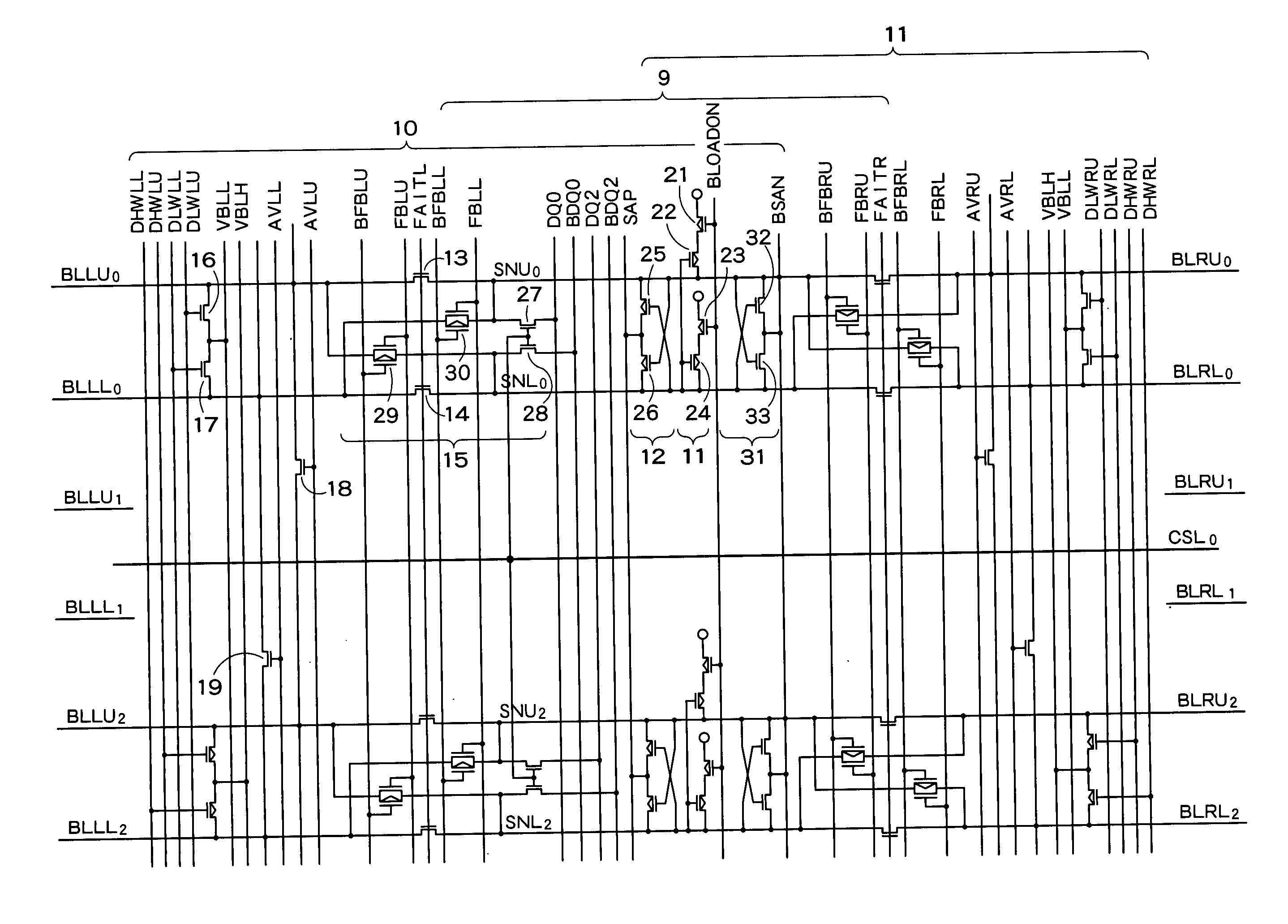
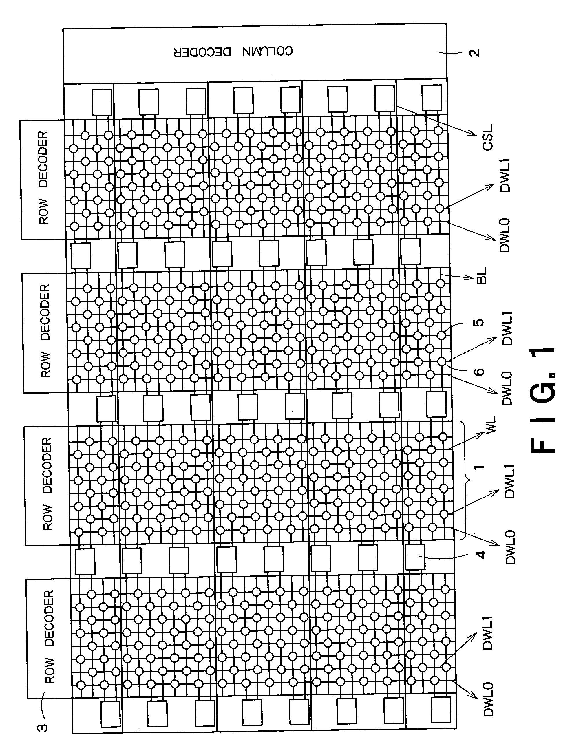
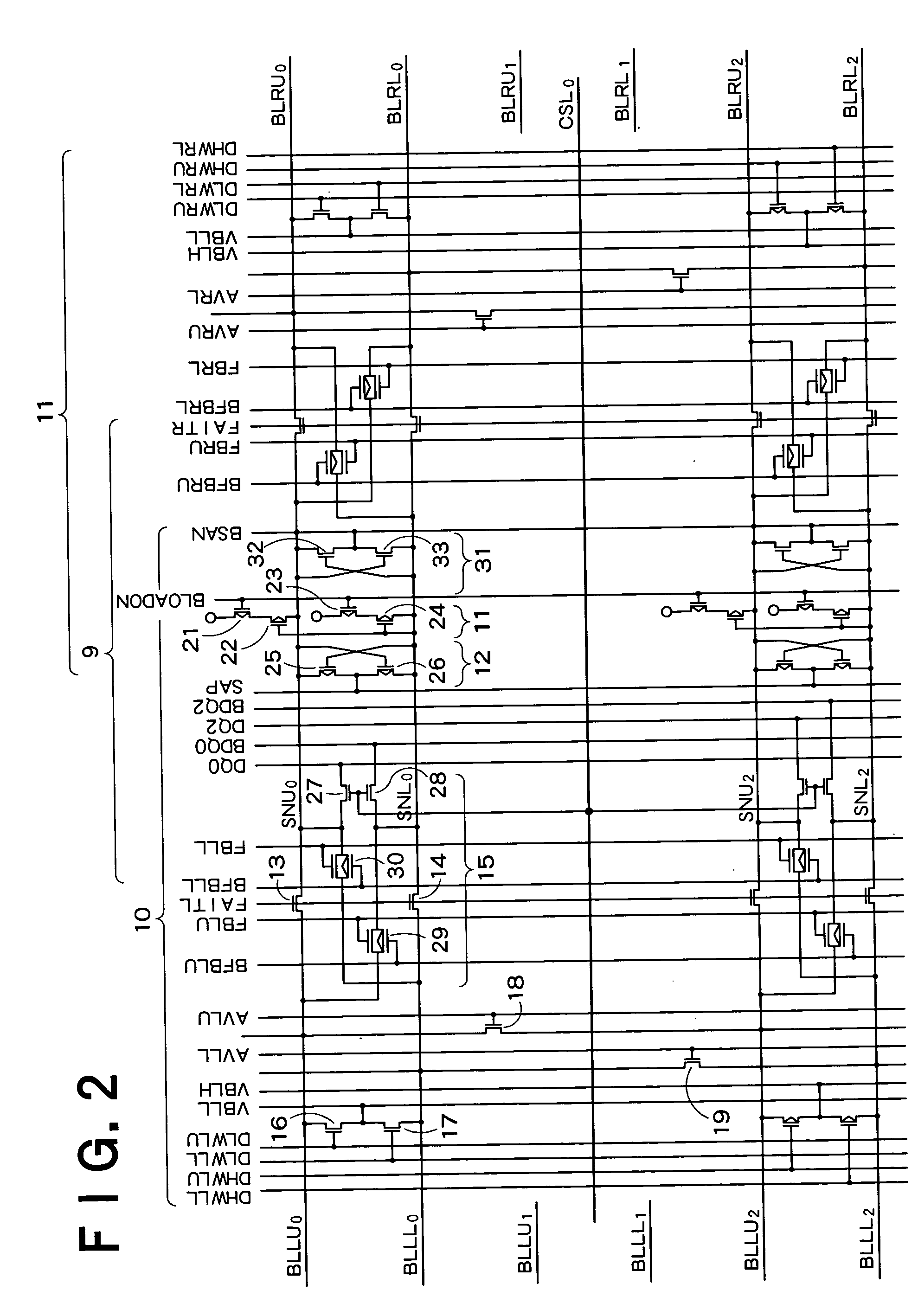
[0016]FIG. 1 is an array configuration of a semiconductor storage device according to a first embodiment of the present invention. The semiconductor apparatus shown in FIG. 1 includes a plurality of cell arrays 1, a column decoder 2 provided corresponding to the cell arrays, row decoders 3 provided for respective cell arrays 1, and double-end type sense amplifiers 4 provided between cell arrays 1 and on both sides of cell arrays 1.

[0017] Each cell array 1 includes a plurality of bit lines BL arranged in the column direction, a plurality of word lines WL arranged in the row direction, two dummy word lines DWL0 and DWL1, FBCs 5 each disposed near at the intersection of a bit line BL and a word line WL, and dummy cells 6 disposed near at the intersection of a bit line and a dummy word line.

[0018] The dummy cells 6 are the same as the FBCs 5 in size, shape and electric characteristics. Data “0” and data “1” are alternately written into the dummy cells 6 for respectiv...

second embodiment

(Second Embodiment)

[0042] In a second embodiment, sense operation is conducted without using the dummy cells 6.

[0043]FIG. 4 is an array configuration diagram of an FBC 5 memory according to the second embodiment of the present invention. In the FBC 5 memory shown in FIG. 4, only FBCs 5 are provided, and dummy cells 6 do not exist. A reference voltage VREF is input to all sense amplifiers 4 from the outside of the array.

[0044]FIG. 5 is a circuit diagram showing an example of an internal configuration of the sense amplifier 4 in the second embodiment. In FIG. 5, components common to those shown in FIG. 2 are denoted by like characters, and hereafter mainly different points will be described.

[0045] The sense amplifier 4 shown in FIG. 5 has transistors 41 and 42 for setting each bit line to a reference potential VREF. Instead, the transistors for short-circuiting bit lines shown in FIG. 2 do not exist.

[0046] The reference potential VREF is an intermediate potential between VBLL and ...


PUM


Abstract

A semiconductor storage device according to one embodiment of the present invention, comprising: FBCs (Floating Body Cells) which store data by accumulating a majority carrier in a floating channel body; and sense amplifiers which perform control reading out data stored in said FBC, wherein each of said sense amplifier includes: a pair of sense nodes provided corresponding to a bit line pair to which said FBC is connected; a pair of load which flow currents through said pair of sense nodes; latch circuits which latch potentials of said pair of sense nodes when a potential difference between said pair of sense nodes reaches a predetermined value; and an output control circuit which outputs latched outputs of said latch circuits at a predetermined timing and feeds back the latched outputs to said bit line pair side to again write it into said FBC.

Description

CROSS REFERENCE TO RELATED APPLICATIONS [0001] This application claims benefit of priority under 35USC§119 to Japanese Patent Application No. 2004-120628, filed on Apr. 15, 2004, the entire contents of which are incorporated by reference herein. BACKGROUND OF THE INVENTION [0002] 1. Field of the Invention [0003] The present invention relates to a semiconductor storage device including FBCs (Floating Body Cells), each of which stores data by storing majority carriers in a channel body of a FET on a semiconductor layer, which is formed on a substrate via an insulation film. [0004] 2. Background Art [0005] As for a conventional DRAM cell including one transistor and one capacitor having a trench capacitor or a stacked capacitor, there is a concern that its fabrication becomes difficult as it becomes finer. As a memory cell that can replace the DRAM cell of this kind, a new memory cell FBC, which stores information by storing majority carriers in a floating body of a FET formed on SOI (...

Claims


Application Information

Patent Timeline
Patent Type & Authority Applications(United States)
IPC IPC(8): G11C11/409G11C11/34
CPCG11C11/4076G11C2211/4016G11C11/4097G11C11/4091
Inventor OHSAWA, TAKASHI
Owner KK TOSHIBA
Why Eureka
Try Eureka