Eureka AIR delivers breakthrough ideas for toughest innovation challenges, trusted by R&D personnel around the world.

Flip chip semiconductor package for testing bump and method of fabricating the same

Inactive Publication Date: 2005-11-10
SAMSUNG ELECTRONICS CO LTD
View PDF7 Cites 19 Cited by
  • Summary
  • Abstract
  • Description
  • Claims
  • Application Information

AI Technical Summary

Problems solved by technology

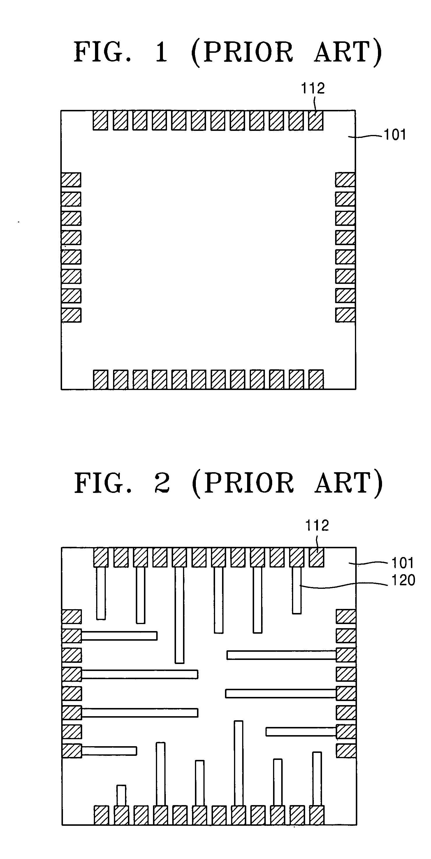
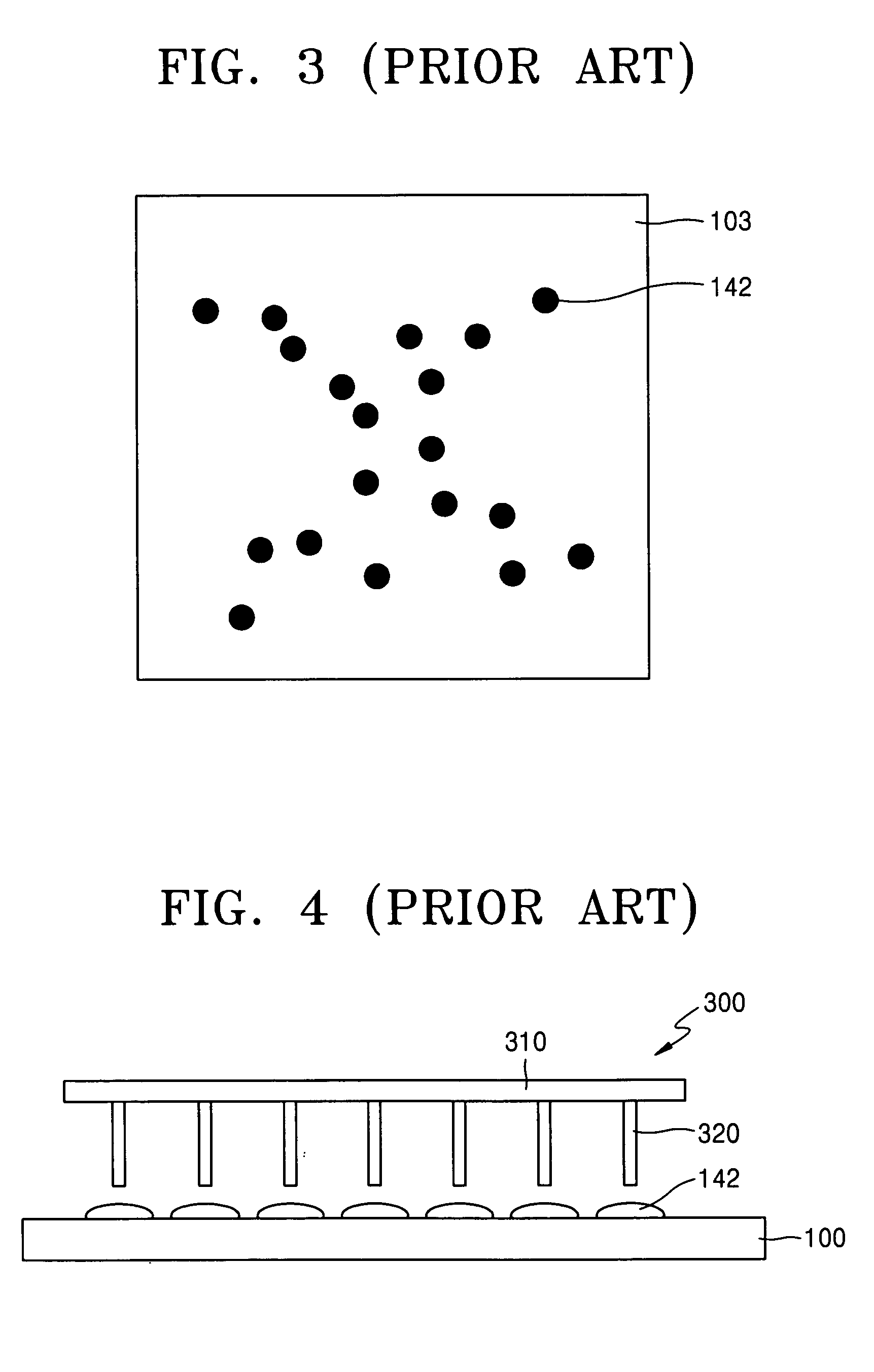
When the vertical probe card 300 is used for the EDS test the manufacturing cost of the flip chip semiconductor package can be increased because the vertical probe card 300 is expensive.
When the conventional probe card is used for the EDS test, the flip chip package can be contaminated because the flip chip package needs to be transferred to a test line during a package fabrication process.

Method used


Image

  • Flip chip semiconductor package for testing bump and method of fabricating the same
  • Flip chip semiconductor package for testing bump and method of fabricating the same
  • Flip chip semiconductor package for testing bump and method of fabricating the same

Examples


Embodiment Construction

[0022] Exemplary embodiments of the present invention will now be described more fully with reference to the accompanying drawings. The invention may, however, be embodied in many different forms and should not be construed as being limited to the exemplary embodiments set forth herein. Rather, these exemplary embodiments are provided so that this disclosure will be thorough and complete, and will fully convey the concept of the invention to those skilled in the art. In the drawings, the thicknesses of layers and regions are exaggerated for clarity.

[0023]FIGS. 8 and 14 show a flip chip semiconductor package according to an exemplary embodiment of the present invention. The flip chip semiconductor package includes a semiconductor chip 200, an insulating layer 201, lower pads 211, a contact layer 202, upper pads 212, mounting bumps 241, redistribution connecting wires 220, and test bumps 242. The insulating layer 201 is formed on a surface of the semiconductor chip 200, on which lowe...


PUM


Abstract

A semiconductor package comprises a plurality of pads disposed along a surface edge of a semiconductor chip, a plurality of mounting bumps formed on a surface of the semiconductor chip and disposed away from the plurality of pads at a predetermined distance, a plurality of redistribution connecting wires for electrically connecting the plurality of pads to the plurality of mounting bumps, and a plurality of test bumps disposed on the plurality of pads.

Description

BACKGROUND [0001] This application claims priority to Korean Patent Application No. 2004-31357, filed on May 4, 2004, in the Korean Intellectual Property Office, the disclosure of which is incorporated herein in its entirety by reference. [0002] 1. Technical Field [0003] The present disclosure relates to a semiconductor package and a method of fabricating the same, and more particularly, to a flip chip semiconductor package for testing a bump and a method of fabricating the same. [0004] 2. Discussion of Related Art [0005] The number of input / output terminals of a semiconductor device becomes increased as integration of the semiconductor device increases. A surface-mount type package becomes used more often than a pin-insertion type package because a number of outer leads that can be formed on a circuit board are limited in the pin-insertion type package. Package methods such as a ball grid array (BGA) package and a chip scale package are proposed to dispose a semiconductor chip in a...

Claims


Application Information

Patent Timeline
IPC IPC(8): H01L21/66H01L21/60H01L23/02H01L23/48H01L23/58
CPCH01L22/32H01L24/10H01L2224/13099H01L2924/01004H01L2924/01015H01L2924/01078H01L2924/01079H01L24/13H01L2924/01082H01L2924/01006H01L2924/01033H01L2924/014H01L2924/00H01L2224/13H01L2224/05011H01L2224/05022H01L2224/05548H01L2224/05567H01L2924/00014H01L2224/0392H01L24/05H01L2224/023H01L2224/05599H01L2224/05099H01L2924/0001H01L22/00
Inventor JUNG, JIN-KOOKBAE, YONG-TAEKIM
Owner SAMSUNG ELECTRONICS CO LTD
Why Eureka
Eureka Blog
Learn More