Method of controlling page buffer having dual register and circuit thereof

Inactive Publication Date: 2005-11-17
STMICROELECTRONICS SRL +1
View PDF7 Cites 3 Cited by
  • Summary
  • Abstract
  • Description
  • Claims
  • Application Information

AI Technical Summary

Benefits of technology

[0013] Accordingly, the present invention has been made in view of the above problems, and it is an object of the present invention to provide a method of controlling a

Problems solved by technology

However, there is a problem in that a transfer time needed for transmitting data from the cache

Method used


Image

  • Method of controlling page buffer having dual register and circuit thereof
  • Method of controlling page buffer having dual register and circuit thereof
  • Method of controlling page buffer having dual register and circuit thereof

Examples


Example

[0020] Now the preferred embodiments according to the present invention will be described with reference to the accompanying drawings. Since preferred embodiments are provided for the purpose that the ordinary skilled in the art are able to understand the present invention, they may be modified in various manners and the scope of the present invention is not limited by the preferred embodiments described later. Further, in the drawing, like reference numerals are used to identify the same or similar parts.

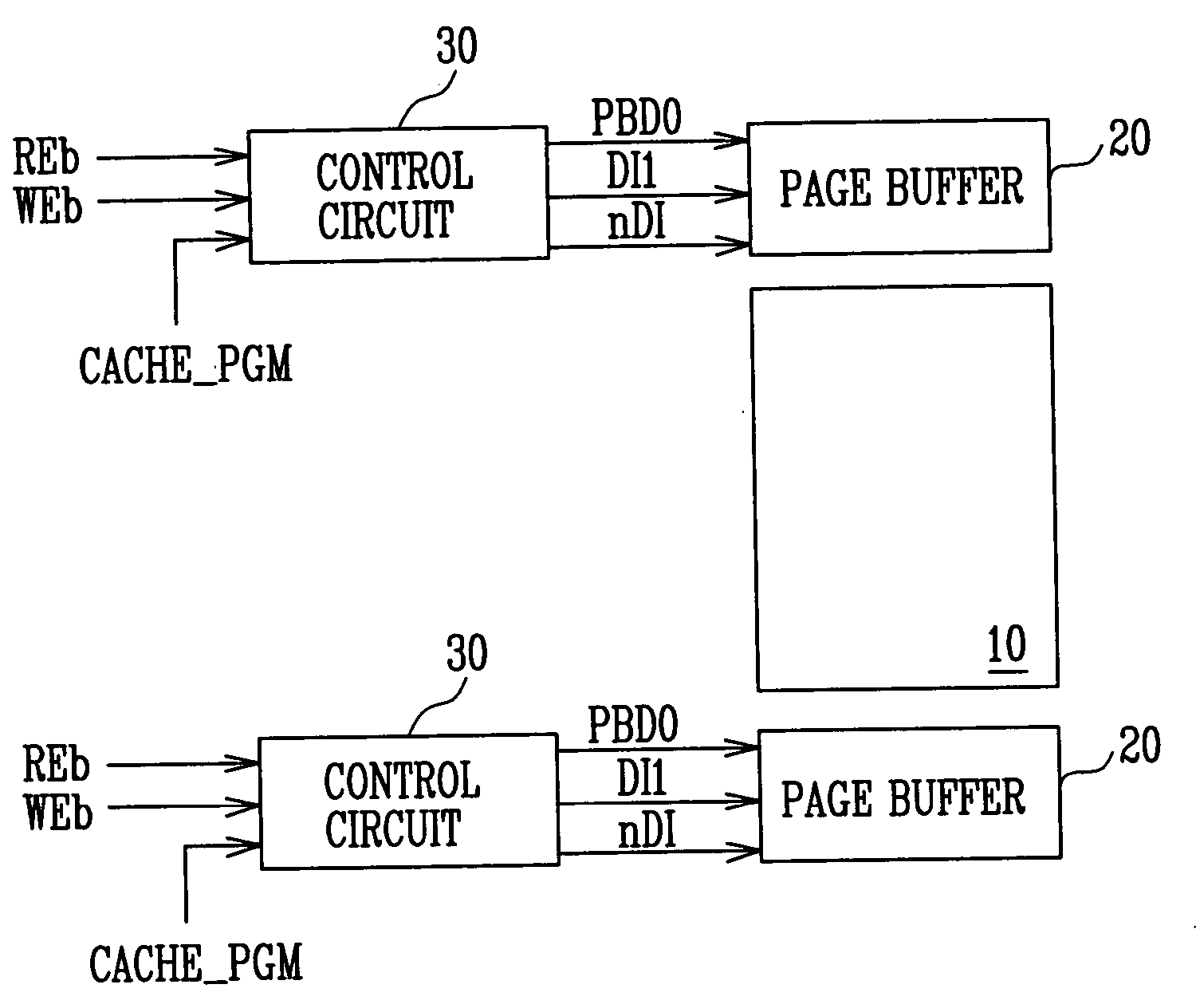
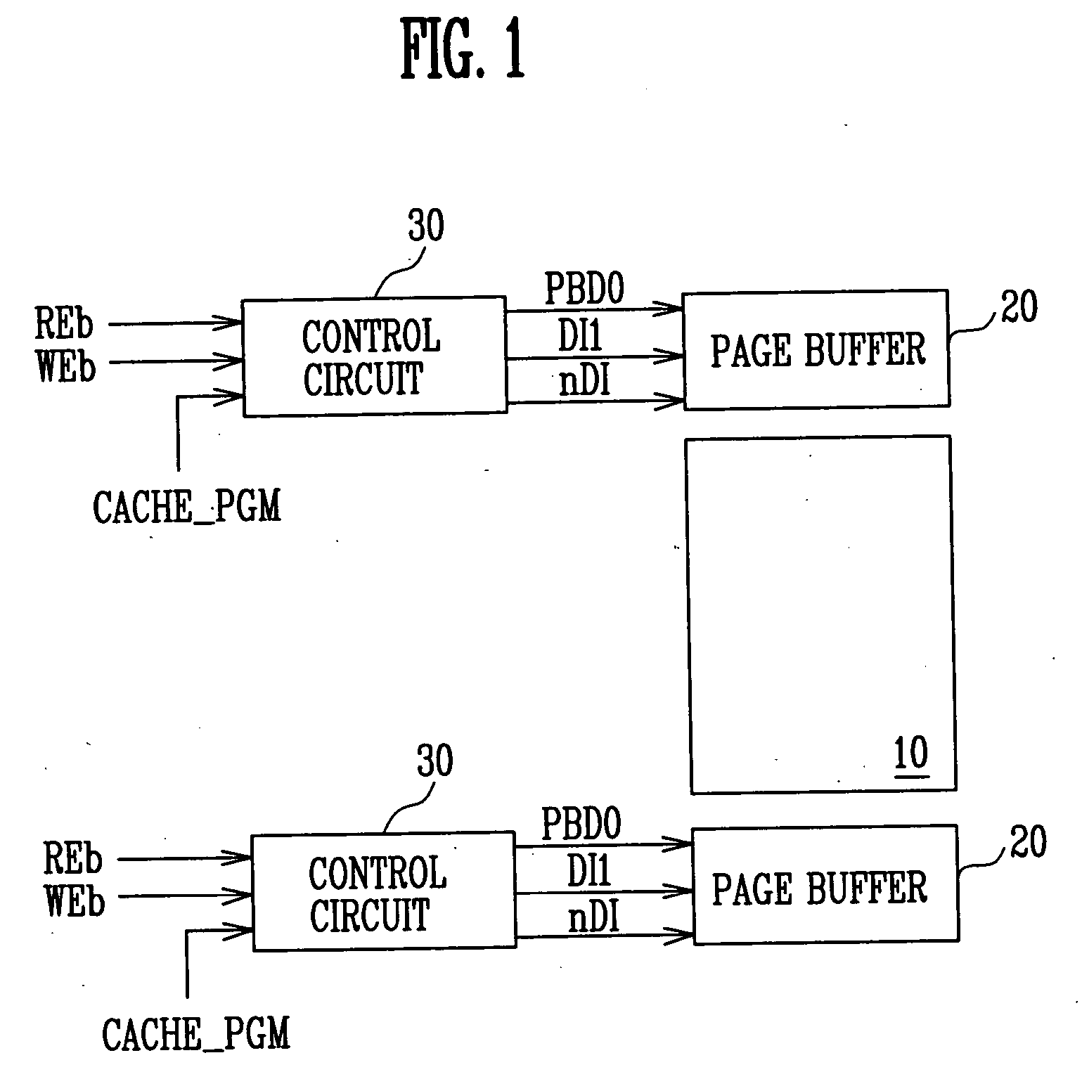
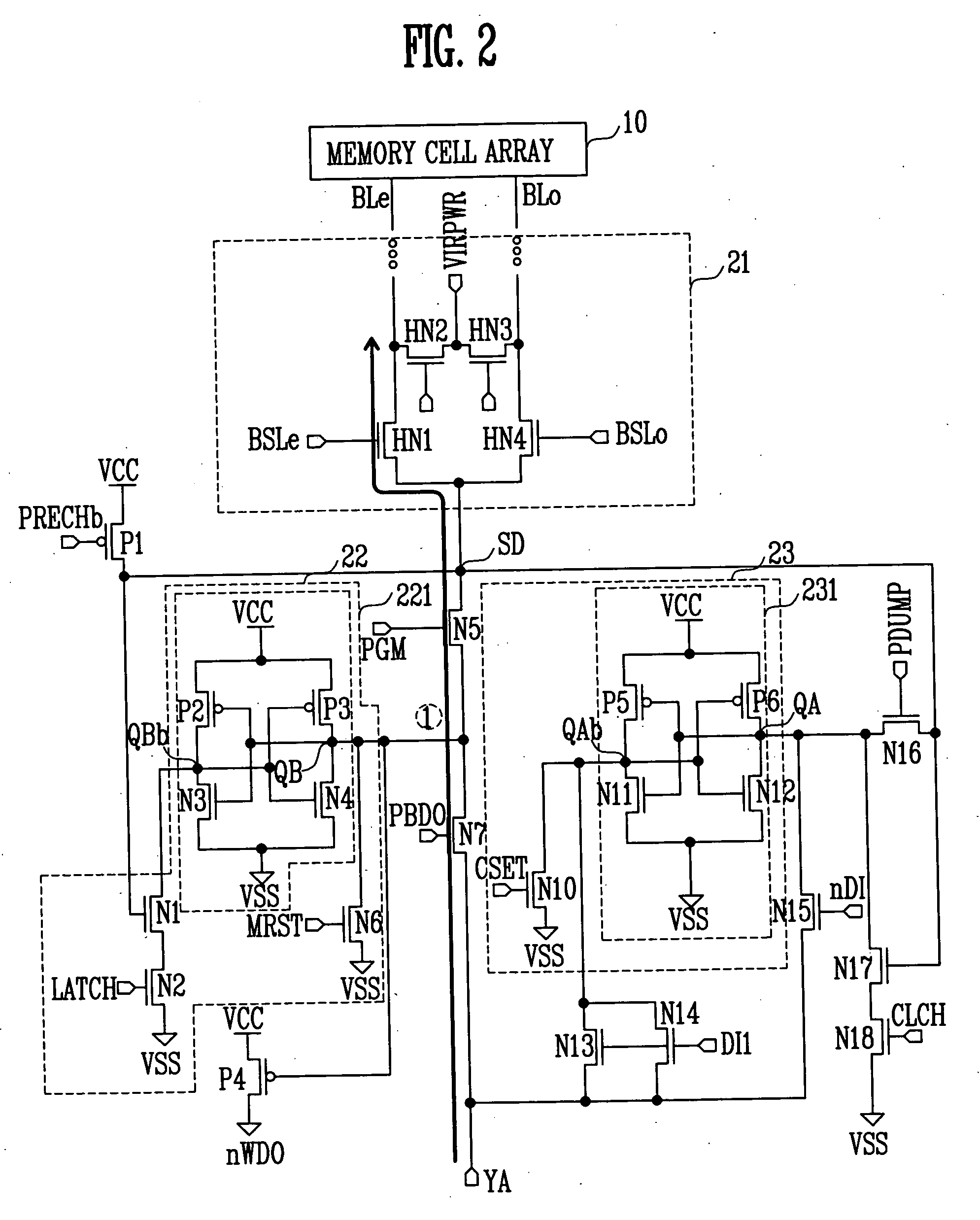
[0021]FIG. 1 shows the construction of a semiconductor memory device that is shown to explain a method of controlling a page buffer having a dual register according to a preferred embodiment of the present invention. FIG. 2 shows the construction of the page buffer shown in FIG. 1. FIG. 3 shows the construction of the control circuit shown in FIG. 1. In FIG. 2, the same reference numerals as those shown in FIG. 4 have the same function. Thus, detailed description on them will be o...


PUM


Abstract

Disclosed are a method of controlling a page buffer having a dual register and a control circuit thereof. In the present invention, during a normal program operation, a normal program operation is performed through the same transmission path as a data transmission path along which data is outputted from bit lines of a memory cell array to a YA pad according to a signal PBDO used in a read operation. A program operating time can be reduced and the whole program operation of a chip can be thus reduced. It is also possible to reduce current consumption by shortening a data path during the normal program operation.

Description

BACKGROUND [0001] 1. Field of the Invention [0002] The present invention relates to a method of controlling a page buffer having a dual register and a control circuit thereof. More specifically, the present invention relates to a method of controlling a page buffer having a dual register in which the entire program time can be reduced through reduction in a program time upon normal program, and a control circuit thereof. [0003] 2. Discussion of Related Art [0004] Recently, there is an increasing demand for semiconductor memory devices that can be electrically programmed and erased and do not require a refresh function to rewrite data in a predetermined period. Further, in order to develop a large-capacity memory device in which lots of data can be stored, researches has been actively made into high-integration technology of the memory device. In the above, the program refers to an operation for writing data into a memory cell and the erasure refers to an operation for erasing data w...

Claims


Application Information

Patent Timeline
IPC IPC(8): G11C16/02G11C7/10G11C11/34G11C16/00G11C16/10
CPCG11C7/1021G11C2216/14G11C16/10
Inventor KIM, EUI SUK
Owner STMICROELECTRONICS SRL
Why Eureka
Try Eureka