Eureka AIR delivers breakthrough ideas for toughest innovation challenges, trusted by R&D personnel around the world.

Method and apparatus of driving a plasma display panel

Inactive Publication Date: 2005-12-22
LG ELECTRONICS INC
View PDF3 Cites 1 Cited by
  • Summary
  • Abstract
  • Description
  • Claims
  • Application Information

AI Technical Summary

Benefits of technology

[0013] An object of the present invention is to provide a method and apparatus for driving a PDP, in which a difference in brightness between blocks is minimized when a screen is driven with it being divided into two or more blocks.
[0016] According to the present invention, in the case where a screen is driven with it being divided into two or more blocks, a difference in brightness between the blocks can be minimized in such a way that an address start time point between the blocks is made different as much as a time interval which is set so that a difference in brightness between the blocks is not shown. Further, according to the present invention, flicker, etc., which is shown when two blocks are driven in the same manner without a time interval, can be prevented.

Problems solved by technology

However, if the whole scan lines SC1 to SCn of the PDP are driven in a so-called ‘ADS (Address & Display Separated)’ mode in which an address period and a sustain period are separated from each other as shown in FIG. 2, there is a problem in that an image cannot be displayed with high brightness and high picture quality since the sustain period is reduced due to an increased address period.
If one of the blocks operates as the sustain period within the same screen during a predetermined period while the other of the blocks operates as the address period, there is a problem in that brightness within the same one screen is different.
In this method, however, there is a problem in that flicker is generated since the emission center point is located at the same time point every frame.

Method used


Image

  • Method and apparatus of driving a plasma display panel
  • Method and apparatus of driving a plasma display panel
  • Method and apparatus of driving a plasma display panel

Examples


Embodiment Construction

[0025] Preferred embodiments of the present invention will be described in a more detailed manner with reference to the drawings.

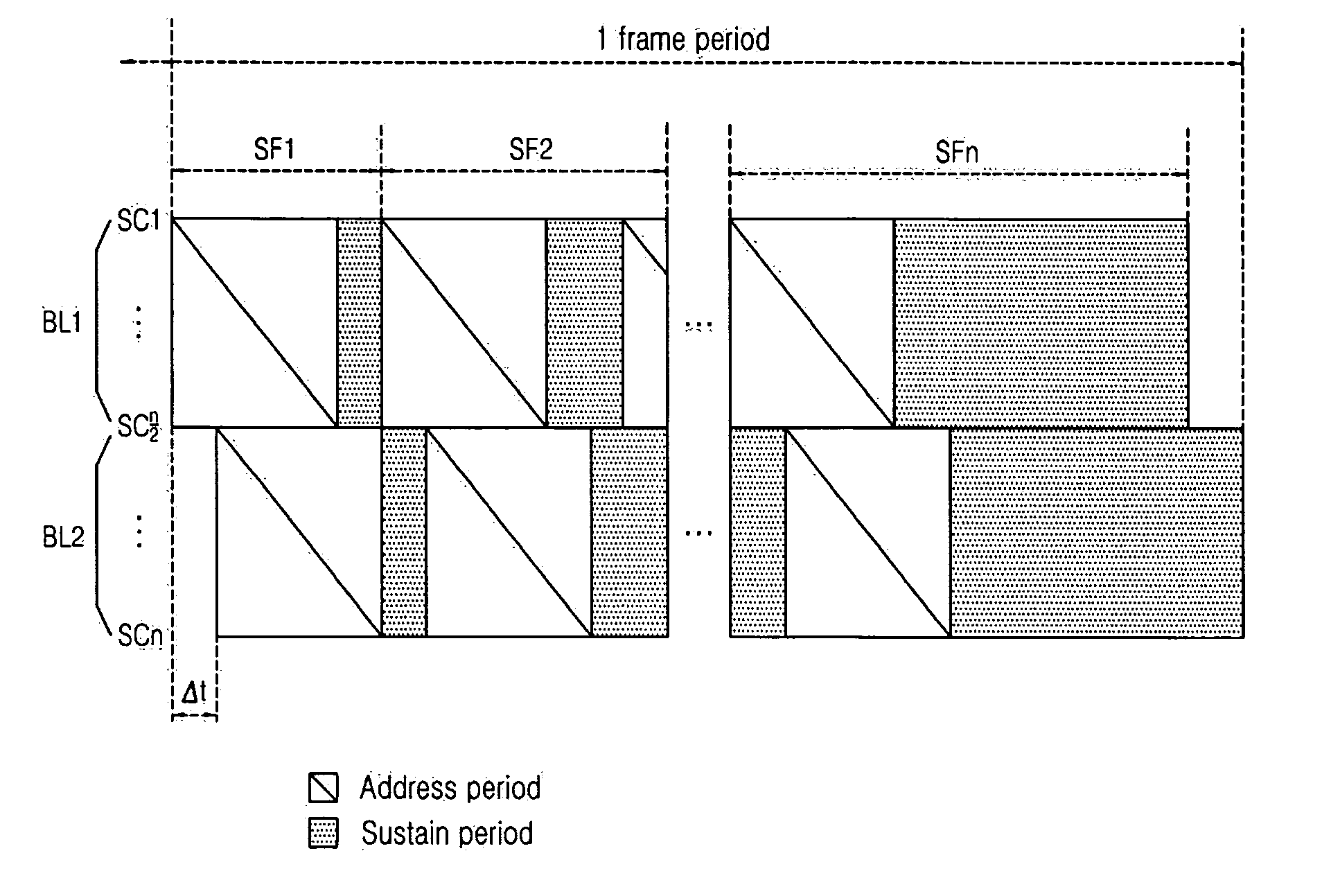
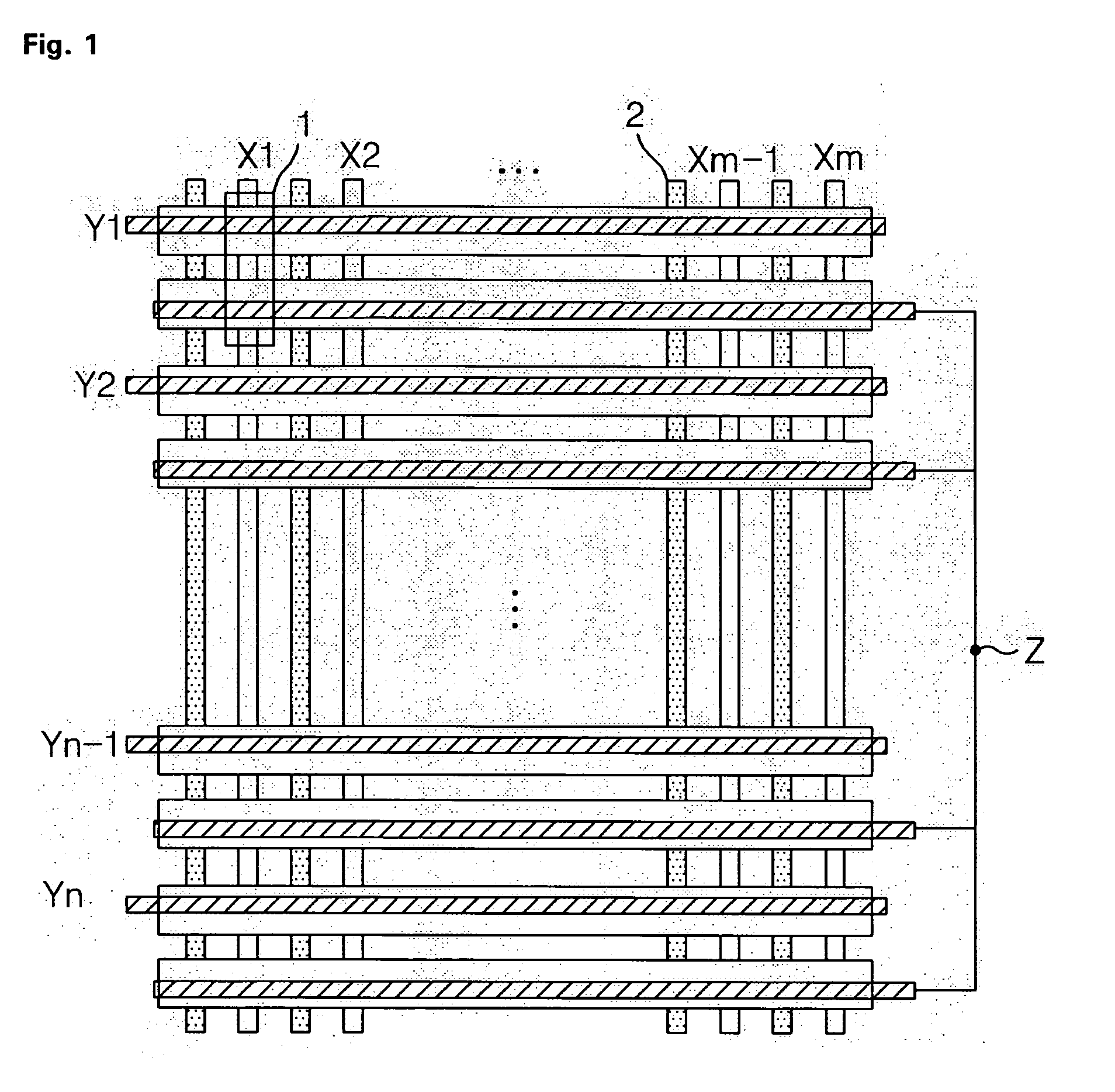
[0026] According to an embodiment of the present invention, there is provided a method of driving a PDP, including the steps of dividing a screen into two or more blocks, and performing an address in the first block of the blocks and then performing an address in the second block of the blocks.

[0027] A time interval between an address start of the first block and an address start of the second block is set to be within a range between 0 and 5 ms.

[0028] The step of performing the address further includes the steps of supplying data to data electrodes of the first block and simultaneously supplying a scan pulse to scan electrodes of the first block, and supplying data to the data electrodes of the second block which are separated from the data electrodes of the first block and simultaneously supplying the scan pulse to the scan electrodes of the second bl...


PUM


Abstract

The present invention relates to a plasma display panel, and more particularly, to a method and apparatus of driving a plasma display panel. According to an embodiment of the present invention, the method includes the steps of dividing a screen into two or more blocks, and performing an address in the first block of the blocks and then performing an address in the second block of the blocks, wherein a time interval between an address start of the first block and an address start of the second block ranges from 0 to 5 ms. Therefore, in the case where a screen is driven with it being divided into two or more blocks, a difference in brightness between the blocks can be minimized in such a way that an address start time point between the blocks is made different as much as a time interval which is set such that a difference in brightness between the blocks is not shown. Further, according to the present invention, flicker, etc., which is shown when two blocks are driven in the same manner without a time interval, can be prevented.

Description

[0001] This Nonprovisional application claims priority under 35 U.S.C. § 119(a) on Patent Application No. 10-2003-0078878 filed in Korea on Nov. 8, 2003, the entire contents of which are hereby incorporated by reference. BACKGROUND OF THE INVENTION [0002] 1. Field of the Invention [0003] The present invention relates to a plasma display panel, and more particularly, to a method and an apparatus of driving a plasma display panel. [0004] 2. Description of the Background Art [0005] A plasma display panel (hereinafter, referred to as a ‘PDP’) is adapted to display an image by light-emitting phosphors with ultraviolet generated during the discharge of a gas such as He+Xe, Ne+Xe or He+Ne+Xe. This PDP can be easily made thin and large, and it can provide greatly increased image quality with the recent development of the relevant technology. Particularly, a three-electrode AC surface discharge type PDP has advantages of lower driving voltage and longer product lifespan as a wall charge is a...

Claims


Application Information

Patent Timeline
IPC IPC(8): G09F9/313G09G3/20G09G3/28G09G3/288G09G3/291G09G3/293G09G3/296G09G3/298H01J17/49
CPCG09G3/288G09G2320/0233G09G2310/0218G09G2310/0205G09G3/293G09G3/296G09G3/294
Inventor PARK, JOONG SEO
Owner LG ELECTRONICS INC
Why Eureka
Eureka Blog
Learn More