
Three-dimensional semiconductor device provided with interchip interconnection selection means for electrically isolating interconnections other than selected interchip interconnections
a three-dimensional semiconductor and interconnection technology, applied in semiconductor devices, digital storage, instruments, etc., can solve the problems of reducing the capacitance of through-via themselves, the difficulty of accurately forming through-holes in chips with a high aspect ratio, and the limit to miniaturization of semiconductors, so as to achieve high-speed operation and reduce power consumption, the effect of reducing the capacitance of interconnections
- Summary
- Abstract
- Description
- Claims
- Application Information
AI Technical Summary
Benefits of technology
Problems solved by technology
Method used
Image

Examples
first embodiment
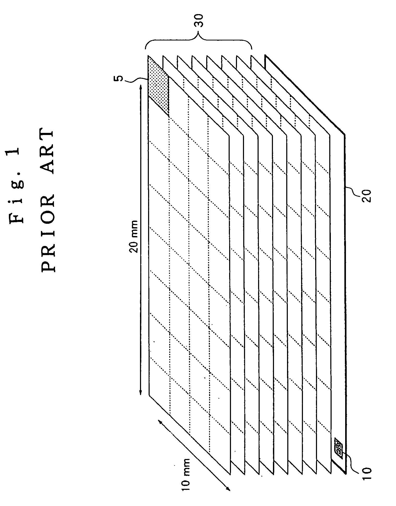
[0045]FIG. 6 shows the configuration of a three-dimensional semiconductor DRAM device, which is a three-dimensional semiconductor device according to the first embodiment of the present invention. In this three-dimensional semiconductor DRAM device, eight memory cell array chips 31 are stacked over interface chip 20 in which circuits for interfacing with the outside are integrated. Memory cell array 63 of 128 Mb, column decoder 61, and row decoder 60 are formed on each memory cell array chip 31.
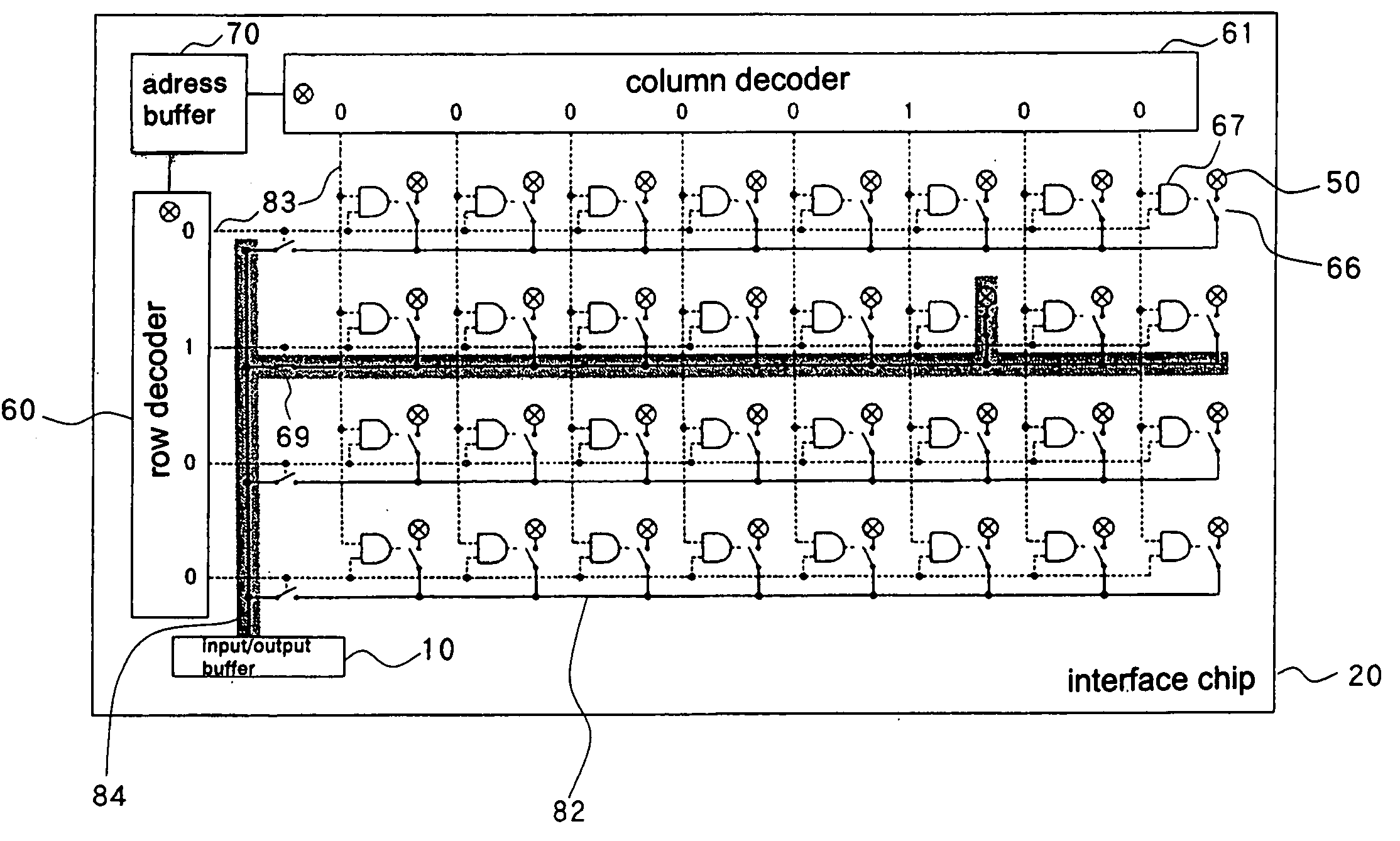
[0046] Interface chip 20 is provided with a circuit for selecting interchip interconnections, a decoder for controlling this circuit, an address buffer, and input / output buffer 10.
[0047] Memory cell array 63 of each memory cell array chip 31 is composed of a plurality of sub-memory arrays 62 of 4 Mb obtained by dividing memory cell array 63 into eight columns and four rows for a total of 32 sub-memory arrays 62. Each sub-memory array 62 is connected to interface chip 20 by way of a respecti...
second embodiment
[0062] The following explanation regards the second embodiment of a three-dimensional semiconductor device according to the present invention. In the present embodiment, the present invention is applied to a three-dimensional DRAM semiconductor device having a multibank configuration.
[0063]FIG. 9 shows the three-dimensional semiconductor DRAM device that is the second embodiment of the present invention, memory cell array chips 72 each having four banks and the selection of interchip interconnections being carried out when selecting banks. In a multibank configuration, memory cells are accessed by designating addresses in bank units, whereby, when accessing a memory cell of a particular bank, interleaving can be carried out in other banks, this interleaving including precharging operations, or further, operations for selecting word lines and activating bit lines, or refresh operations, and banks can therefore be accessed one after another and data transferred continuously.
[0064] I...
PUM
 Abstract
Description
Claims
Application Information