Bipolar transistor with geometry optimized for device performance, and method of making same

a bipolar transistor and geometry technology, applied in the field of bipolar transistors, can solve the problems of device failure, limiting the performance capability of the device, and bipolar transistors consuming a relatively large amount of silicon area

Inactive Publication Date: 2006-01-12
MICROSEMI SEMICON U S
View PDF7 Cites 4 Cited by
  • Summary
  • Abstract
  • Description
  • Claims
  • Application Information

AI Technical Summary

Benefits of technology

[0008] The present invention is generally directed to various embodiments of a bipolar transistor with the geometry optimized for device performance and various methods of making same. In one illustrative embodiment, the device comprises a substrate, an intrinsic base region formed in the substrate, a continuous emitter region formed withi

Problems solved by technology

Such current crowding may limit the performance capability of the device and, in some cases, result in device failure.
However

Method used


Image

  • Bipolar transistor with geometry optimized for device performance, and method of making same
  • Bipolar transistor with geometry optimized for device performance, and method of making same
  • Bipolar transistor with geometry optimized for device performance, and method of making same

Examples


Embodiment Construction

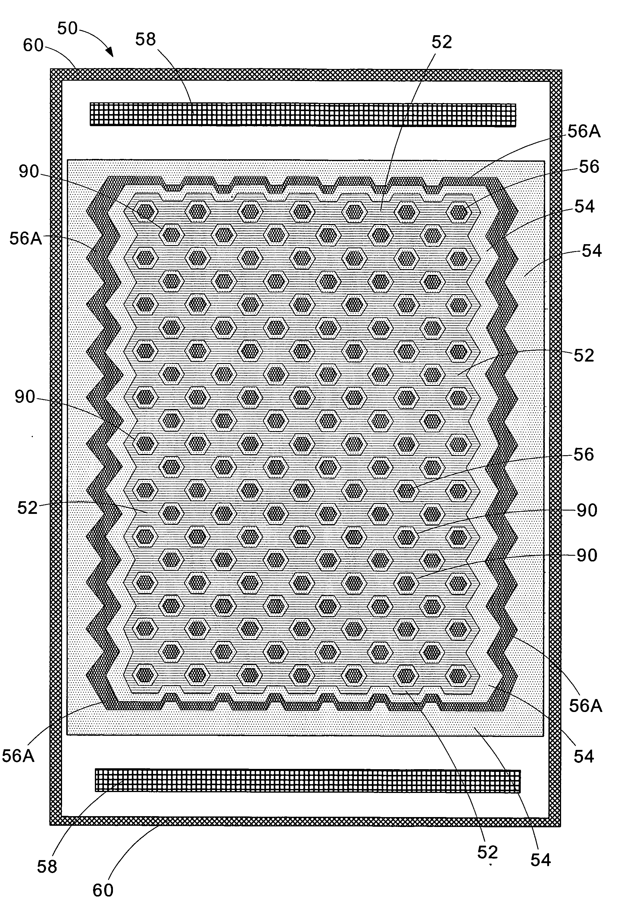
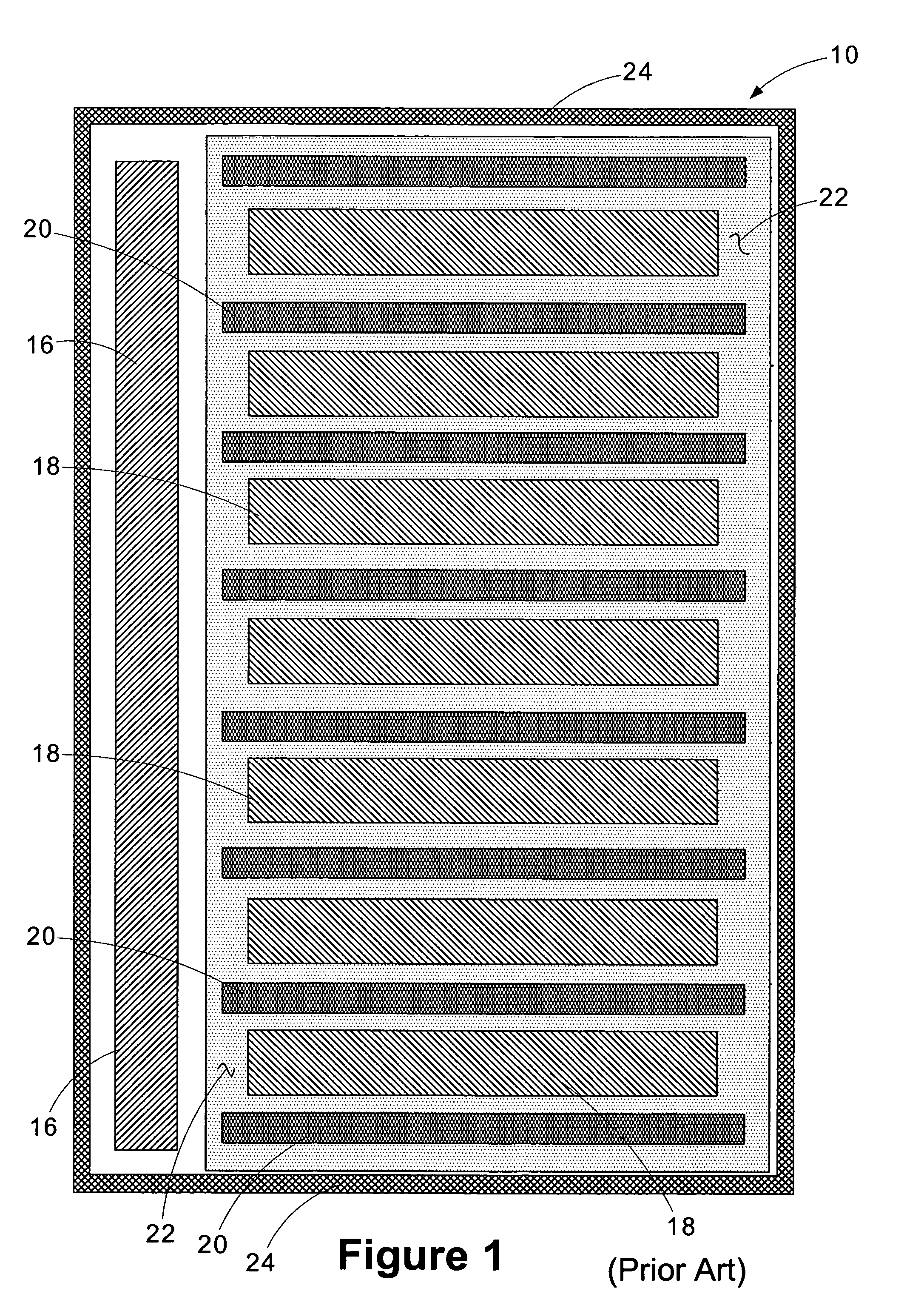
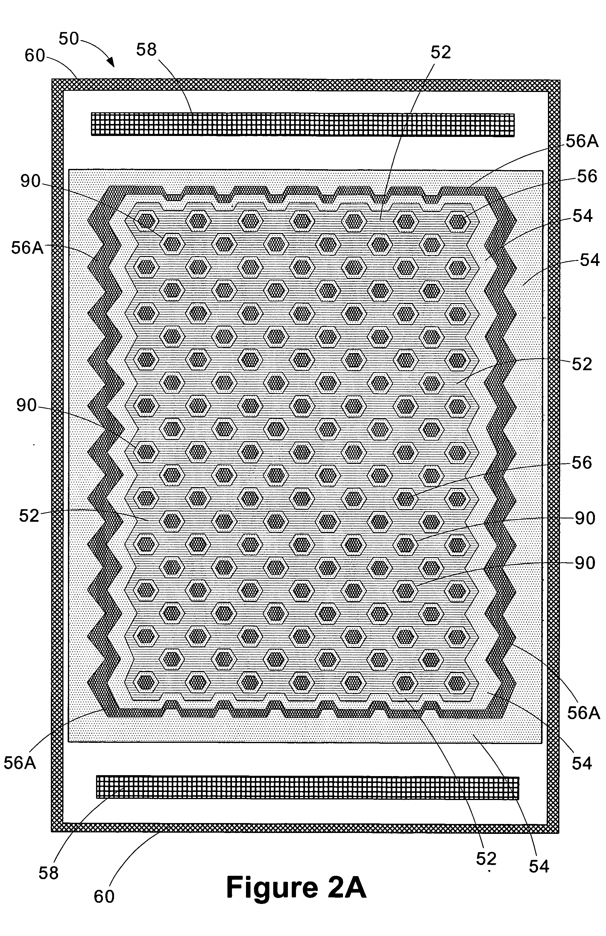
[0019] Illustrative embodiments of the invention are described below. In the interest of clarity, not all features of an actual implementation are described in this specification. It will of course be appreciated that in the development of any such actual embodiment, numerous implementation-specific decisions must be made to achieve the developers' specific goals, such as compliance with system-related and business-related constraints, which will vary from one implementation to another. Moreover, it will be appreciated that such a development effort might be complex and time-consuming, but would nevertheless be a routine undertaking for those of ordinary skill in the art having the benefit of this disclosure.

[0020] The present invention will now be described with reference to the attached figures. Although the various layers, doped regions and structures of the semiconductor devices are depicted in the drawings as having very precise, sharp configurations and profiles, those skille...


PUM


Abstract

The present invention is generally directed to bipolar transistors with geometry optimized for device performance and various methods of making same. In one illustrative embodiment, the device includes a substrate, an intrinsic base region formed in the substrate, a continuous emitter region formed within the intrinsic base region, the emitter region having a plurality of substantially hexagonal shaped openings defined therein, and a plurality of extrinsic base regions formed in the substrate, wherein each of the extrinsic base regions is positioned within an area defined by one of the plurality of substantially hexagonal shaped openings.

Description

BACKGROUND OF THE INVENTION [0001] 1. Field of the Invention [0002] This invention is generally related to the field of semiconductor devices, and, more particularly, to a bipolar transistor with geometry optimized for device performance and a method of making same. [0003] 2. Description of the Related Art [0004] There is a constant drive within the semiconductor industry to increase the operating efficiency and reduce the size of bipolar junction transistors and integrated circuit devices incorporating such transistors. This drive is fueled by demands for electronic devices that operate at increasingly greater speeds, consume less power, and an overall desire for more physically compact devices. Power bipolar transistors are employed in a variety of integrated circuit devices. For example, such power bipolar transistors may be employed in a typical ADSL line driver or in a subscriber line interface card (SLIC) which are in widespread use in the telecommunications industry. Such pow...

Claims


Application Information

Patent Timeline
IPC IPC(8): H01L27/082
CPCH01L29/73H01L29/0692
Inventor DUTTA, RANADEEP
Owner MICROSEMI SEMICON U S
Why Eureka
Try Eureka