Process for resurf diffusion for high voltage MOSFET

Active Publication Date: 2006-01-12
INFINEON TECH AMERICAS
View PDF6 Cites 6 Cited by
  • Summary
  • Abstract
  • Description
  • Claims
  • Application Information

AI Technical Summary

Benefits of technology

[0015] By employing the ultra shallow implanted N buffer region in the P substrate, it was found that there is a much better distribution and contr

Problems solved by technology

This causes the diffusion 23 to occupy a relatively large portion of the total chip area, reducing the useful area of the various junction-containing wells.
Furthermore, the thicker epitaxial layer 10

Method used


Image

  • Process for resurf diffusion for high voltage MOSFET
  • Process for resurf diffusion for high voltage MOSFET
  • Process for resurf diffusion for high voltage MOSFET

Examples


Example

DETAILED DESCRIPTION OF THE DRAWINGS

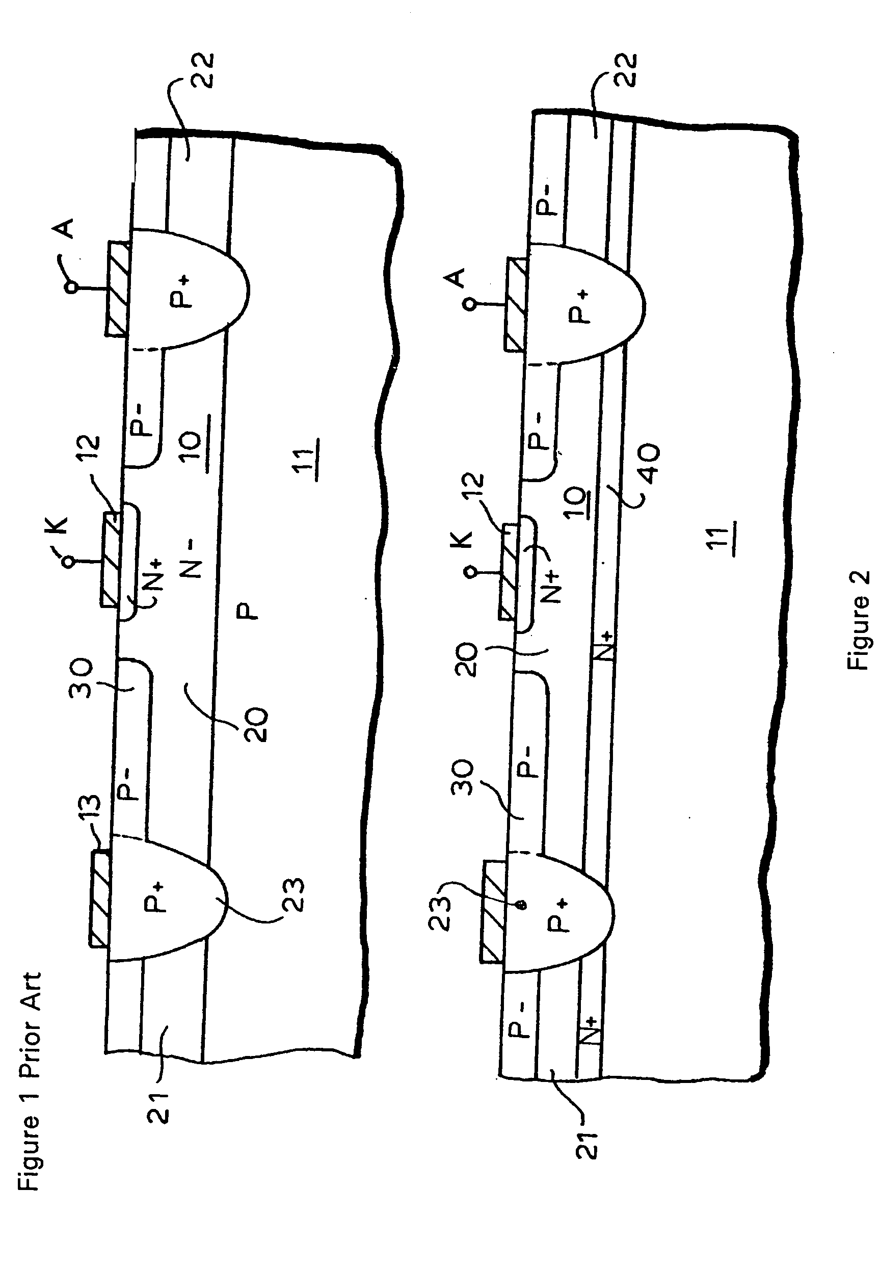
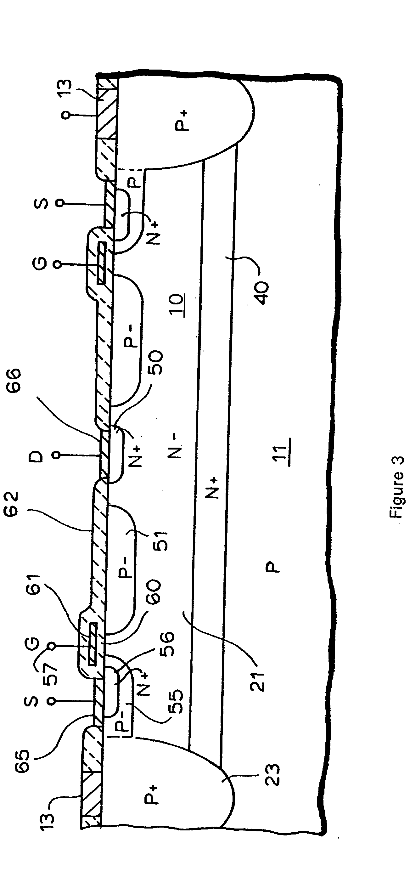
[0024] (a) The Prior Art

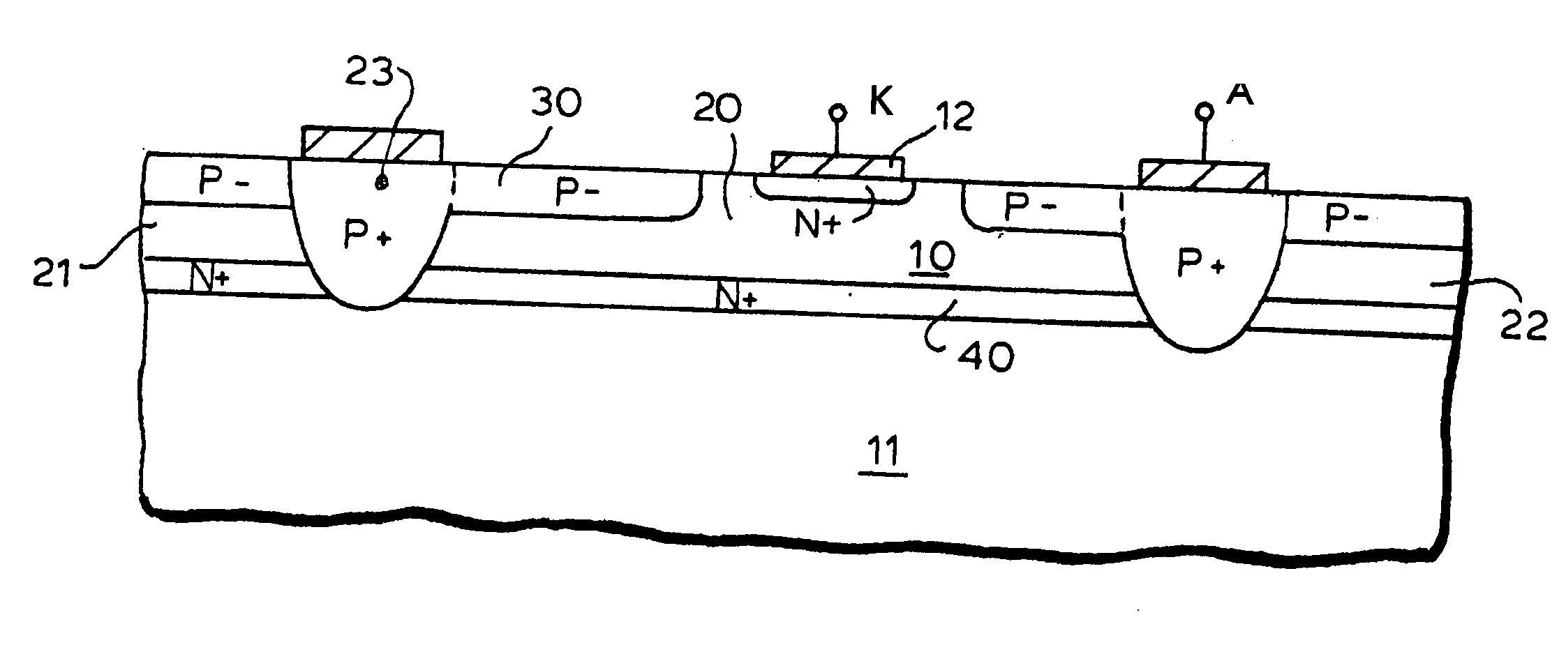
[0025] Referring first to FIG. 1, there is shown a prior art, horizontal conduction diode, the junctions of which are formed in an N− well 10 of an N− epitaxial layer of monocrystalline silicon, deposited atop a P type substrate 11. An N+ diffusion provides a low resistance contact to cathode electrode 12 having terminal “K”. Ring-shaped electrode 13 is the device anode “A”.

[0026] The epitaxial layer 10 (sometimes termed “epi”) is divided into a plurality of isolated wells 20, 21 and 22 as by one or more P type isolation diffusions such as diffusion 23 which may be ring-shaped in topology, but can have any other desired topology. Anode contact 13 is deposited atop P+ region 23. Diffusion 23 must be deep enough to intercept the P / N boundary between regions 10 and 11 in order to isolate regions or wells 20, 21 and 22. Wells 21 and 22 may contain any desired junction pattern, forming diodes, MOSgated devices and / or bipolar ...


PUM


Abstract

A starting wafer for high voltage semiconductor devices is formed by implanting arsenic into the top surface of a p type silicon substrate wafer to a depth of about 0.1 micron. A N type non-graded epitaxial layer is then grown atop the substrate without any diffusion step so that the arsenic is not intentionally driven. Device junction are then diffused into the epitaxially grown layer.

Description

FIELD OF THE INVENTION [0001] This invention relates to semiconductor device processing and more specifically relates to a novel process for manufacture of and structure for silicon wafers which are to be used in the fabrication of semiconductor devices. BACKGROUND OF THE INVENTION [0002] It is common in semiconductor device fabrication to form an epitaxially-deposited silicon junction-receiving layer atop a silicon wafer. The epitaxial layer will have a low concentration of N or P impurities while the substrate is a thicker and higher concentration layer. Any desired type of junction pattern is then formed in the epitaxial layer to form known devices such as MOSFETs, IGBTs, diodes, integrated circuits, and the like. [0003] High voltage semiconductor devices commonly employ a resurf region which is a low concentration region between areas of high potential difference. The resurf region depletes as the voltage difference increases, and is fully depleted before the maximum voltage dif...

Claims


Application Information

Patent Timeline
IPC IPC(8): H01L29/739
CPCH01L29/0634H01L29/0878H01L29/1083H01L29/1087H01L29/1095H01L2924/0002H01L29/7816H01L29/8611H01L2924/00H01L29/739
Inventor HERMAN, THOMAS
Owner INFINEON TECH AMERICAS
Why Eureka
Try Eureka