Land grid array terminal having variable circuitry

a technology of variable circuitry and grid array terminal, which is applied in the direction of printed circuits, coupling contact members, coupling device connections, etc., can solve the problems of reducing the depth hb>2/b> affordable for the elastic arm, reducing the length weakening the supporting strength of the elastic arm, etc., to achieve a larger elastic deformation, shorter conducting circuitry, and strong supporting strength

Inactive Publication Date: 2006-02-16
STARLINK ELECTRONICS CORP
View PDF4 Cites 16 Cited by
  • Summary
  • Abstract
  • Description
  • Claims
  • Application Information

AI Technical Summary

Benefits of technology

[0008] Therefore, the objective of the present invention is to provide a land grid array terminal that has stronger supporting strength, shorter conducting circuitry, and can afford larger elastic deformation.
[0009] In light of the above and other objectives, the terminal of the present invention includes a bend portion protrusively formed on the elastic arms of the terminal. When the elastic arms are pressed, the two bend portions of the elastic arms contact each other, resulting in a shorter conducting circuitry. In addition, the contact of the two bend portions forms a structural supporting point, which reduces the inclination angle of the elastic arms and supports a larger elastic deformation. This renders the terminal of the present invention being shorter in conducting circuitry and stronger in supporting strength.

Problems solved by technology

This is disadvantageous for at least the following reasons:
(2) Since the pivotal point of the conventional elastic arm is the base, the supporting strength thereof is often not strong enough when the elastic arm is pressed to a larger deformation.
However, reducing the length of the elastic arm will reduce the depth h2 affordable for the elastic arm.
The insufficient affordable depth of the terminal may result in an unstable electrical contact, especially when the electronic device is warped and deformed.
However, the C-shape terminal 80 is disadvantageous in that the deformation of the terminal 80 can only reach to a depth h3 of 0.18 mm, which is insufficient for securing the electrical conductance.

Method used


Image

  • Land grid array terminal having variable circuitry
  • Land grid array terminal having variable circuitry
  • Land grid array terminal having variable circuitry

Examples


Embodiment Construction

[0015] In order to better understanding the technical features of the present invention, detailed descriptions thereof are hereinafter provided by incorporating with the accompanying drawing.

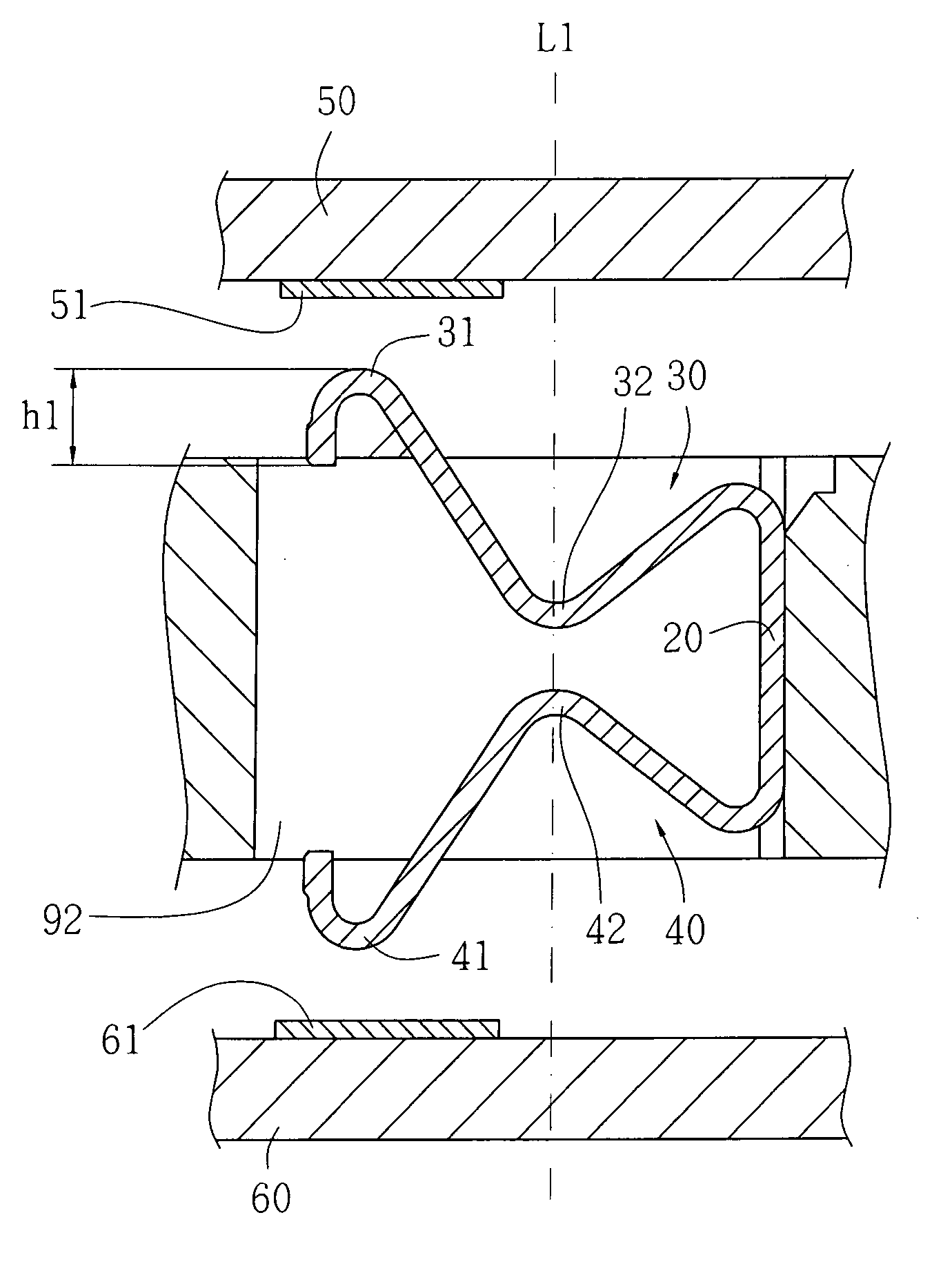
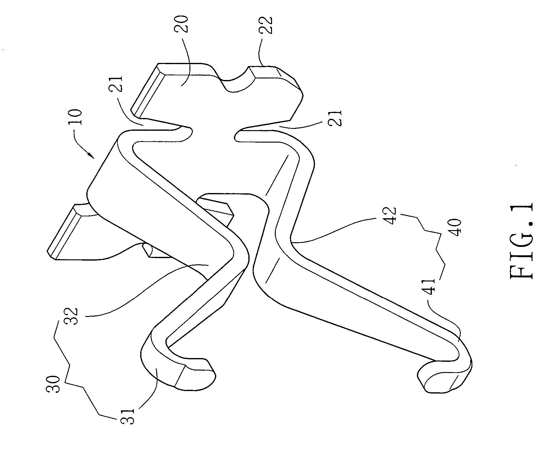
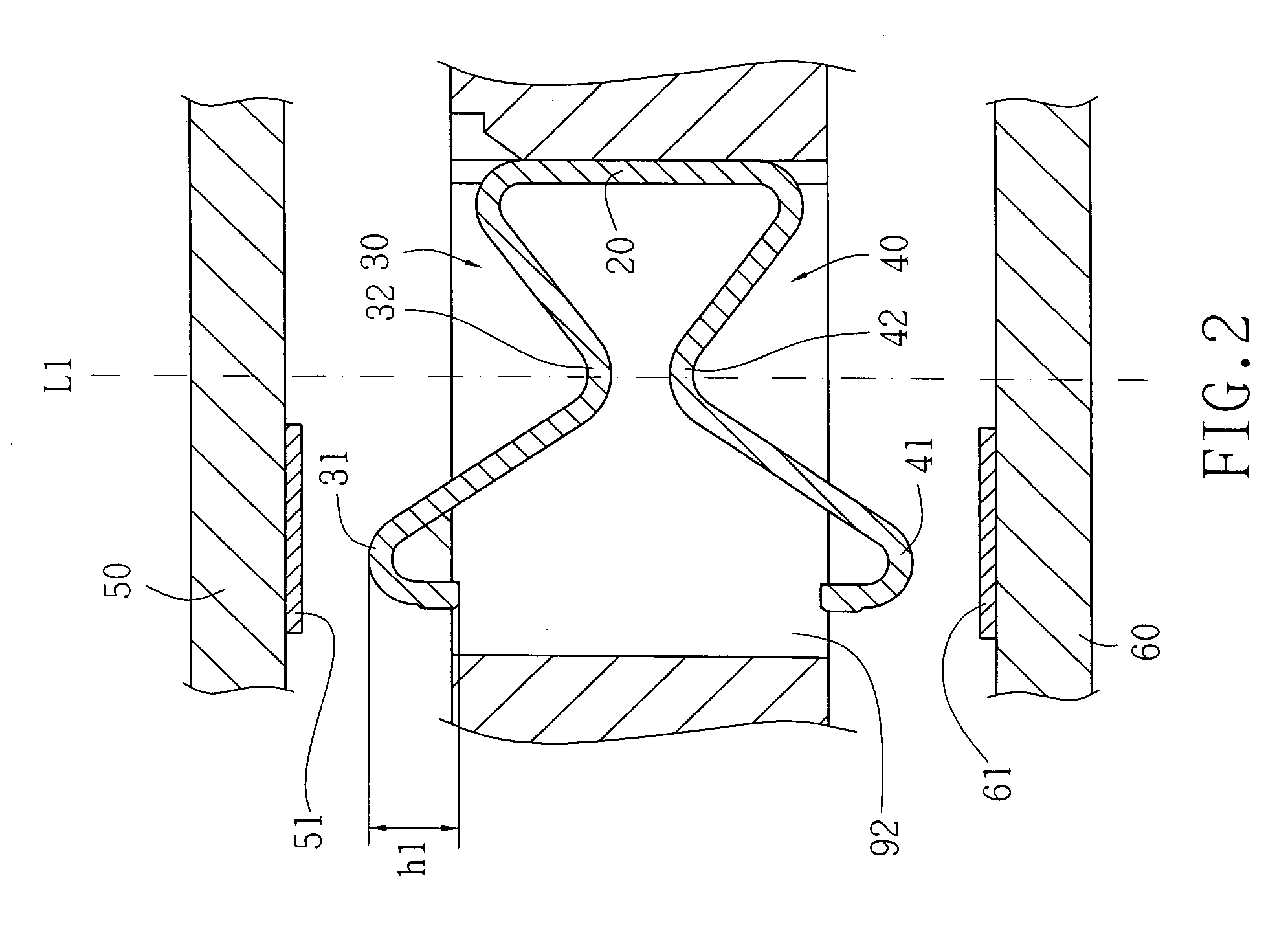
[0016] Referring to FIG. 1 and FIG. 2, the terminal 10 of the present invention is illustrated. The terminal 1 comprises a vertically disposed side plate 20. A barb 22 is formed at both sides of the side plate 20. Two elastic arms 30, 40 are respectively formed on the top portion and the bottom portion of the side plate 20. The elastic arms 30, 40 comprises contact portions 31, 41 respectively at the end portions thereof, and bend portions 32, 42 at the non-contact portions. In this particular embodiment, the bend portions 32, 42 are in a V-shape, while in other embodiments, the bend portions 32, 42 can be any arch shape equivalent to the V-shape as shown and described. In order to enhance the elastic properties of the elastic arms 30, 40, a plurality of concave grooves 21 is formed on the side...


PUM


Abstract

A land grid array terminal is provided. The terminal includes a side plate, and two elastic arms respectively formed on the upper and lower portions of the side plate. At the central portion of the each elastic arm, a bend portion is formed protrusively facing towards each other. The terminal has a larger circuitry when it is not pressed. However, when the terminal is pressed, the bend portions of the elastic arms contact each other to form a shorter circuitry. This renders a shorter conducting circuitry and a better supporting strength.

Description

BACKGROUND OF THE INVENTION [0001] 1. Field of the Invention [0002] The present invention relates generally to a land grid array terminal having a variable circuitry, and more particularly to a land grid array terminal that the elastic arm thereof forms a non-end portion contact when pressing both ends of the terminal, which renders a shorter conducting circuitry and a better supporting strength. 2. Prior Art [0003] Land grid array (LGA) technique is gradually becoming a widely adopted standard in electronic industry. A conventional LGA terminal 70, as shown in FIG. 4, comprises a vertically disposed base 71. Two elastic arms 72, 73 are extensively formed on the upper end and the lower end of the base 71, respectively. The ends of the elastic arms 72, 73 extend outward, contacting an electronic device and a printed circuit board, respectively. In order to make better served elastic arms 72, 73, the two end portions of the base 71 and the ends of the elastic arms 72, 73 must be separ...

Claims


Application Information

Patent Timeline
Patent Type & Authority Applications(United States)
IPC IPC(8): H01R12/00H01R13/00H01R13/24
CPCH01R12/714H01R13/2435
Inventor HSU, WEN-TE
Owner STARLINK ELECTRONICS CORP
Why Eureka
Try Eureka