Optical fiber array

a technology of optical fiber array and optical fiber, applied in the field of optical fiber array, can solve the problems of increasing cost and power consumption, deteriorating optical channel quality, and devices for converting optical and electrical signals, and achieve the effect of small displacement of optical fibers and low cos

Inactive Publication Date: 2006-02-23
NIPPON TELEGRAPH & TELEPHONE CORP
View PDF2 Cites 0 Cited by
  • Summary
  • Abstract
  • Description
  • Claims
  • Application Information

AI Technical Summary

Benefits of technology

[0023] The present invention has been made to solve the above problems, and has as its object to provide a two-dimensional optical fiber array with a small displacement of optical fibers at a low cost.

Problems solved by technology

It is pointed out that such a device for converting optical and electrical signals will greatly increase in cost and power consumption with an improvement in signal bandwidth (see non-patent reference 1: A. S. Morris III, “In search of transparent networks”, IEEE Spectrum, pp.
The light beam that has undergone the optical axis inclination due to the beam-position displacement causes crosstalk between adjacent channels, resulting in a deterioration in optical channel quality.
The influences of the shrinking of an adhesive must be taken into consideration, and it is difficult to control the positions of the substrates in consideration of the shrinking.
However, a manufacturing method using such a high-precision machining technique or process is not suitable for mass production, and hence it is difficult to reduce the manufacturing cost.
(4) Since the outer diameter of an optical fiber is as small as 125 μm, the optical fiber is very difficult to handle.
Since such optical fibers that are difficult to handle are used, it is difficult to reduce the assembly cost for the two-dimensional fiber array 120 shown in FIG. 8.
However, the glass-transition temperature of the thermoplastic resin used for the ferrule 132 is near 180 to 200° C., and hence it is technically difficult to form an anti-reflection coating film by vapor deposition in the presence of the ferrule 132.

Method used


Image

  • Optical fiber array
  • Optical fiber array
  • Optical fiber array

Examples


first embodiment

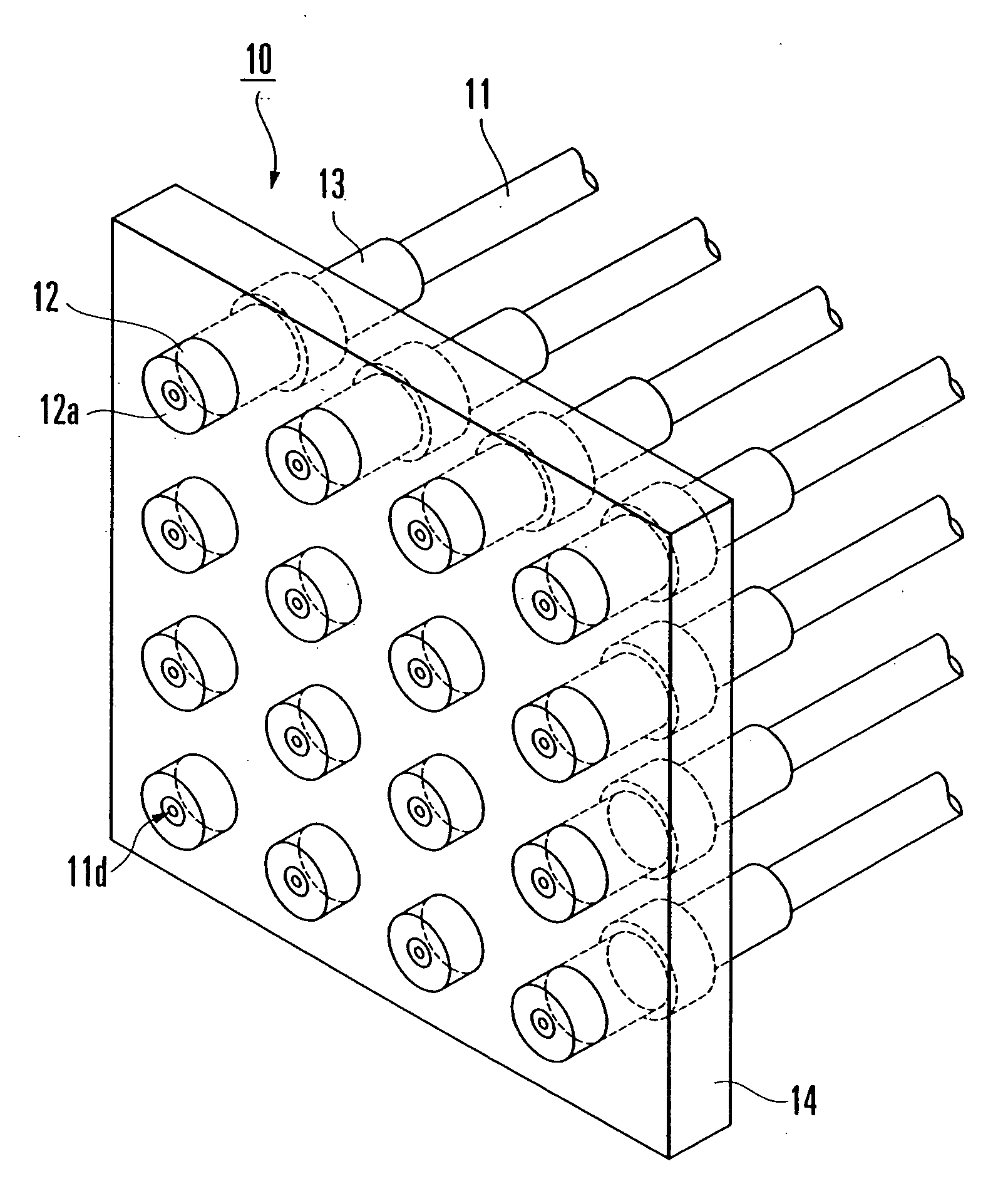
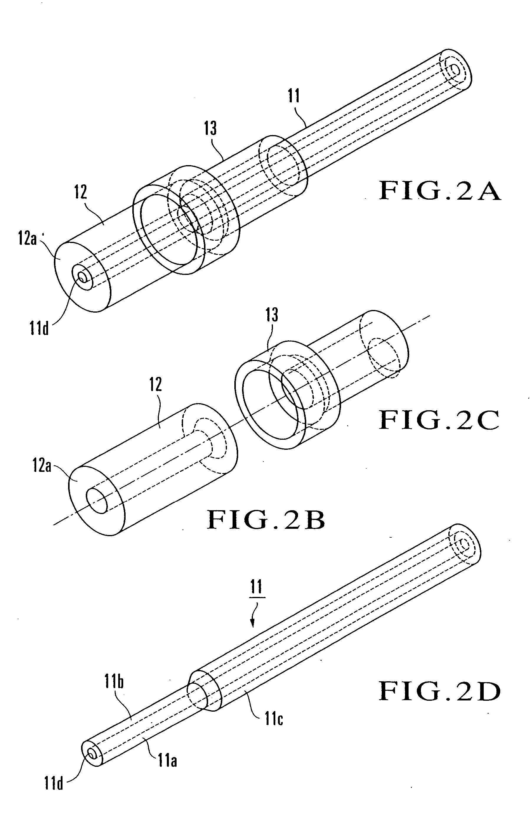
[0035] An optical fiber array according to the first embodiment of the present invention will be described first. FIG. 1 shows the arrangement of an optical fiber array 10 according to this embodiment. The optical fiber array 10 has a plurality of optical fibers 11 arrayed by inserting cylindrical ferrules 12 attached to the distal end portions of the optical fibers 11 into through holes arrayed / formed in an alignment substrate 14. Each optical fiber 11 is fitted in a through hole formed in the central portion of the ferrule 12, and a light incident / exit end face 11d of the optical fiber 11 is exposed on the end face 12a side of the ferrule 12.

[0036] As shown in FIG. 2, a sheath 11c on the distal end portion of the optical fiber 11 is removed, and an exposed waveguide portion constituted by a core 11a and cladding 11b is fitted in the ferrule 12. On the side where the optical fiber 11 is inserted into the ferrule 12, a cylindrical tube 13 for protecting them partly covers the ferru...

second embodiment

[0048] An optical fiber array according to the second embodiment of the present invention will be described next. FIG. 5 shows an alignment substrate 24 as a component of the optical fiber array of this embodiment. The same reference numerals as in the first embodiment denote the same parts in the second embodiment, and a repetitive description will be avoided.

[0049] As shown in FIG. 5, each guide hole 14a of the alignment substrate 24 has one pair of arcuated buffer slits 24b which are formed along the periphery of the guide hole 14a. In addition, notches 24c communicating with the guide hole 14a are formed between the end portions of the pair of buffer slits 24b. When the ferrule 12 shown in FIGS. 1 and 2 is inserted into the guide hole 14a, these buffer slits 24b and notches 24c serve as buffer means.

[0050] The alignment substrate 24 having the buffer slits 24b and the like allows the ferrules 12 to be easily inserted into the guide holes 14a. Assume that the outer diameter of ...

third embodiment

[0054] The third embodiment of the present invention will be described next. FIG. 6 shows an alignment substrate 34 as a component of an optical fiber array according to the third embodiment. The same reference numerals as in the first and second embodiments denote the same parts in the third embodiment, and a repetitive description will be avoided.

[0055] As shown in FIG. 6, the alignment substrate 34 has buffer holes 34c formed along each array of guide holes 14a near the peripheral ends of the alignment substrate 34 in one array direction of the guide holes 14a (the vertical direction in FIG. 6). In addition, the alignment substrate 34 has buffer slits 34b between the adjacent guide holes 14a and between the guide holes 14a and the buffer holes 34c. The buffer slits 34b make these holes communicate with each other. When the ferrules 12 shown in FIGS. 1 and 2 are inserted into the guide holes 14a, the buffer slits 34b and buffer holes 34c serve as buffer means.

[0056] In the align...


PUM


Abstract

An optical fiber array includes an alignment substrate, a plurality of ferrules, and a plurality of optical fibers. The alignment substrate has a plurality of guide holes which are two-dimensionally arrayed and extend through the substrate. The ferrules are respectively inserted into the guide holes in the same direction and have through holes in the central portions. The optical fibers are fitted and held in the respective through holes. The guide hole is formed into a cylindrical shape having a diameter substantially equal to the outer diameter of the ferrule. The light incident / exit end face of the optical fiber is exposed on one end face of the ferrule.

Description

BACKGROUND OF THE INVENTION [0001] The present invention relates to an optical fiber array as a component of an optical switch, an isolator, the input / output portion of an optical connection device, a semiconductor laser, an optical coupling component between a photodiode and an optical fiber, or a multicore optical connector. [0002] With an abrupt increase in data traffic, a strong demand has arisen for an increase in the capacity of a trunk network. In this trunk network, a large-capacity optical network using a WDM (Wavelength Division Multiplexing) technique has already been introduced for data transmission equipment. However, the following scheme is used for a node portion. First, an optical signal is temporarily converted into an electrical signal, and paths are switched by a switch using a conventional electric circuit. Then, the signal is converted into an optical signal again to be returned to the data transmission equipment. [0003] It is pointed out that such a device for ...

Claims


Application Information

Patent Timeline
Patent Type & Authority Applications(United States)
IPC IPC(8): G02B6/00G02B6/35G02B6/36
CPCG02B6/3556G02B6/3582G02B6/3644G02B6/3696G02B6/3672G02B6/3676G02B6/3652
Inventor YAMAMOTO, TSUYOSHIUENISHI, YUJIYAMAGUCHI, JOHJI
Owner NIPPON TELEGRAPH & TELEPHONE CORP
Why Eureka
Try Eureka