

Epitaxial structure and fabrication method of nitride semiconductor device
a technology of nitride semiconductor and epitaxial structure, which is applied in the manufacture of semiconductor/solid-state devices, semiconductor devices, electrical equipment, etc., can solve the problems of inferior device characteristics, short operation life, and large difference between the lattice constant of the substrate and the nitride epitaxial layer,
- Summary
- Abstract
- Description
- Claims
- Application Information
AI Technical Summary
Benefits of technology
Problems solved by technology
Method used
Image

Examples
first embodiment
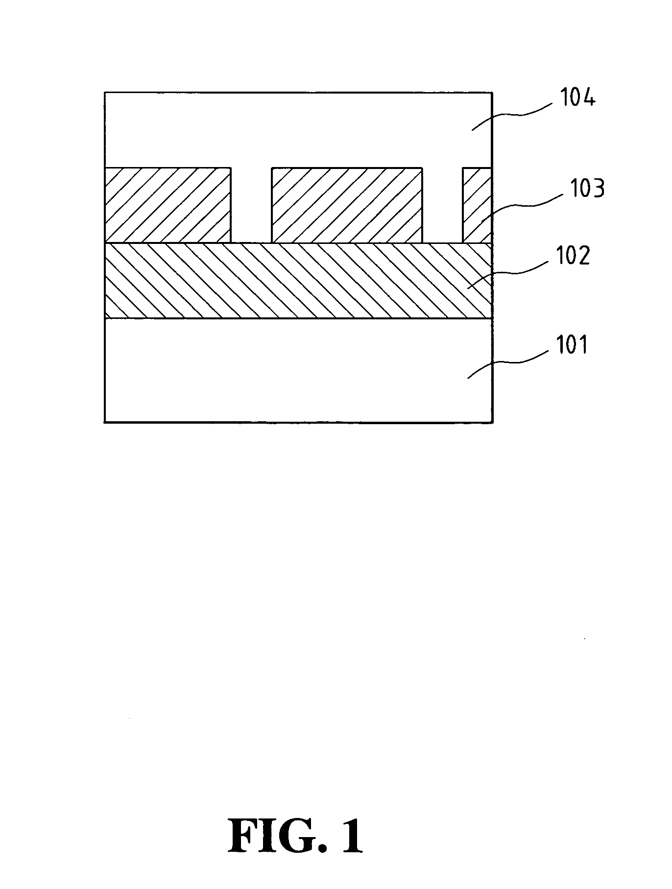
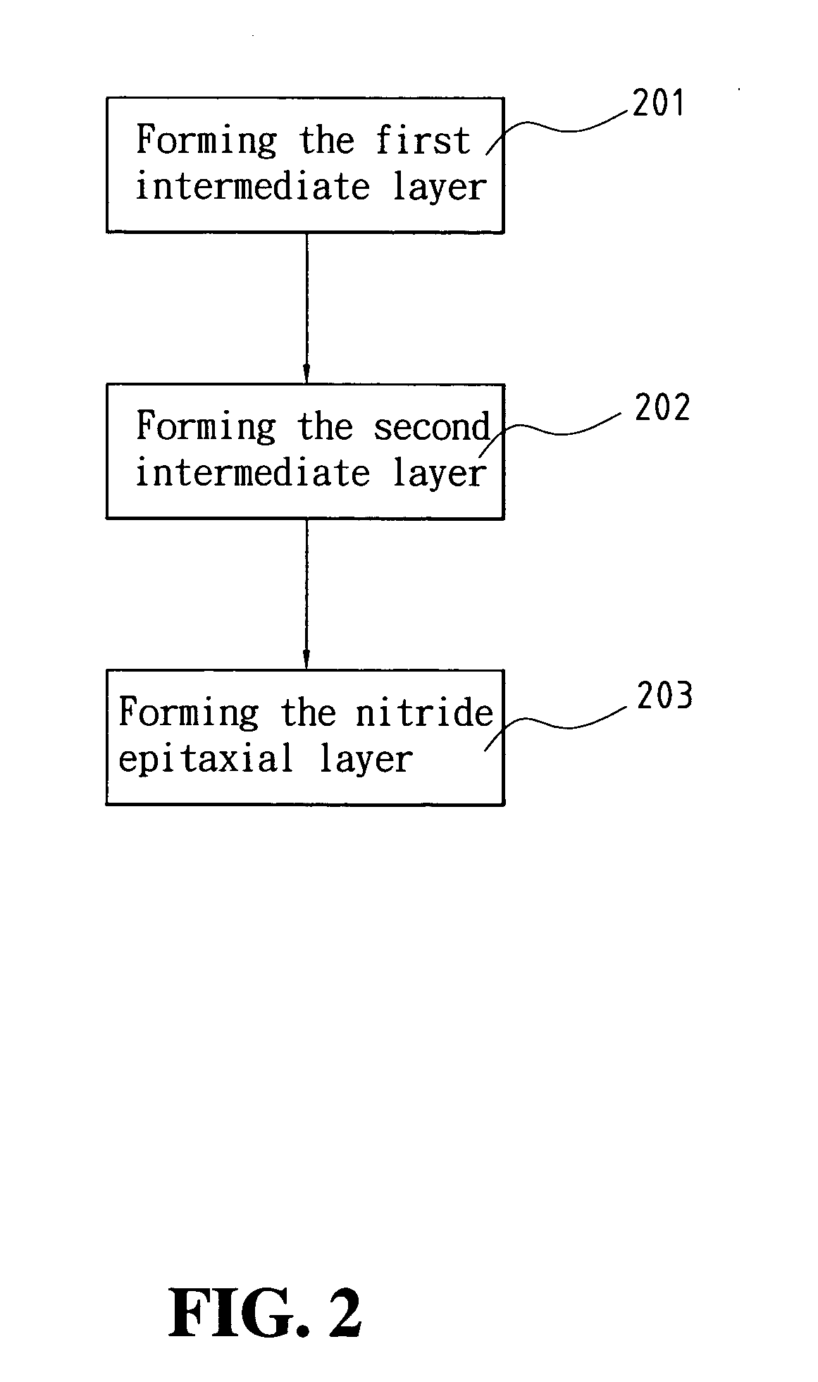
[0017]FIG. 1 is a schematic diagram showing the structure of the nitride semiconductor device according to present invention. FIG. 2 is a flow diagram showing the processing steps for forming the nitride semiconductor device as depicted in FIG. 1. As shown in FIG. 1, the nitride semiconductor device is formed by stacking a first intermediate layer 102, a second intermediate layer 103, and a nitride epitaxial layer 104, sequentially in this order from bottom to top on a substrate 101. The second intermediate layer 103, when deposited, would form a mask having a random, clustered pattern on the first intermediate layer 102. The nitride epitaxial layer 104 subsequent deposited then grows from the exposed first intermediate layer 102 not covered by the mask of the second intermediate layer 103, and overflows to cover the top of the mask of the second intermediate layer 103. The processing steps, as shown in FIG. 2, include: on the substrate 101, forming the first intermediate layer 102 ...
second embodiment
[0020]FIG. 3 is a schematic diagram showing the structure of the nitride semiconductor device according to present invention. As shown in FIG. 3, the nitride semiconductor device contains multiple first and second intermediate layers 102 and 103 stacked alternately upon each other between the substrate 101 and the nitride epitaxial layer 104. More specifically, on the substrate 101, the steps 201 and 202 as depicted in FIG. 2 are performed in sequence to form the first pair of the first and second intermediate layers 102 and 103. But before the step 203 is performed, the steps 201 and 202 are repeated at least once so that additional pairs of the first and second intermediate layers 102 and 103 are formed and stacked upon one another. Each of the first intermediate layers 102 is made of Al1-p-qGapInqN (p, q≧0, 1≧p+q≧0) with a specific composition, and has a thickness between 5 Å and 10 Å. Similarly, each of the second intermediate layers 103 is made of SiaNb (a, b≧0) or MgcNd (c, d≧...
third embodiment
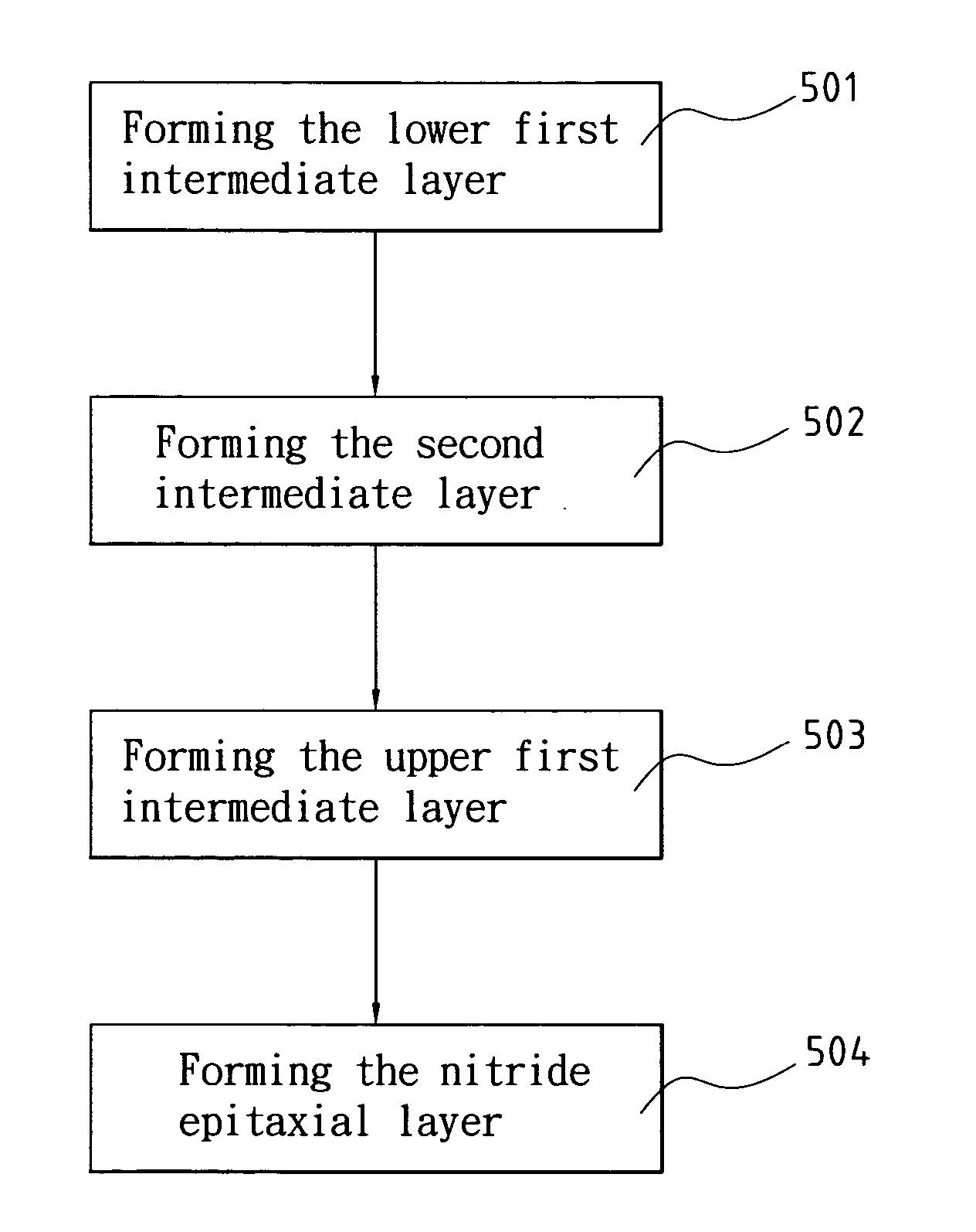
[0022]FIG. 4 is a schematic diagram showing the structure of the nitride semiconductor device according to present invention. FIG. 5 is a flow diagram showing the processing steps for forming the nitride semiconductor device as depicted in FIG. 4. As shown in FIG. 4, the nitride semiconductor device is formed by stacking a lower first intermediate layer 402, a second intermediate layer 403, an upper first intermediate layer 402, and a nitride epitaxial layer 404, sequentially in this order from bottom to top on a substrate 401. The second intermediate layer 403, when deposited, would form a mask having a random, clustered pattern on the lower first intermediate layer 402. The upper first intermediate layer 402 subsequent deposited then grows from the exposed, lower first intermediate layer 402, and overflows to cover the top of the mask of the second intermediate layer 403. The upper first intermediate layer 402 is added to enhance the epitaxial quality of the nitride epitaxial laye...
PUM
 Abstract
Description
Claims
Application Information