

Liquid ejection head, image forming apparatus and method of manufacturing liquid ejection head
- Summary
- Abstract
- Description
- Claims
- Application Information
AI Technical Summary
Benefits of technology
Problems solved by technology
Method used
Image

Examples
first embodiment
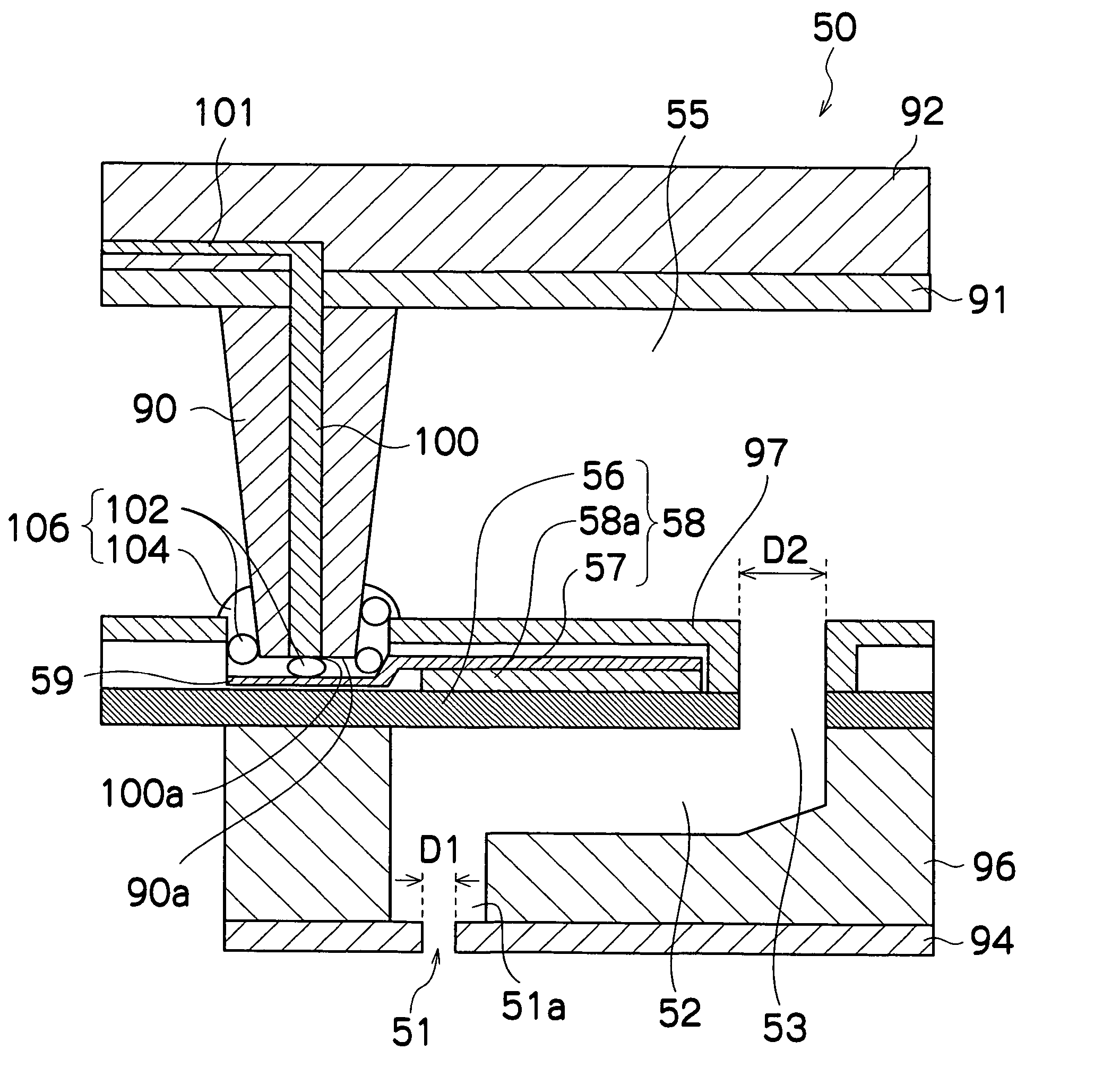
[0147]FIG. 9 is an enlarged diagram of a peripheral area of a bonding section between a piezoelectric element wire 90 and an electrode pad 59 in the present invention.
[0148] The adhesive 106 used for connecting the piezoelectric element wires 90 with the electrode pads 59 is made of a non-conductive resin 104 which contains conductive particles 102. For example, a commercially available epoxy resin, such as anisotropically conductive adhesive, may be used as the adhesive 106. Epoxy-based adhesives have high chemical resistance, and as in the present embodiment, they are suitable for bonding piezoelectric element wires 90 which are soaked in the ink.
[0149] In the present embodiment, the front end 90a of the piezoelectric element wire 90 is bonded to the electrode pad 59 by means of an adhesive 106, as shown in FIG. 9.
[0150] In this case, the front end 100a of the electrode section 100 formed inside each piezoelectric element wire 90 is connected to the electrode pad 59 by means of ...
PUM
 Abstract
Description
Claims
Application Information