USB attach detection for USB 1.1 and USB OTG devices
- Summary
- Abstract
- Description
- Claims
- Application Information
AI Technical Summary
Benefits of technology
Problems solved by technology
Method used
Image
Examples
Embodiment Construction
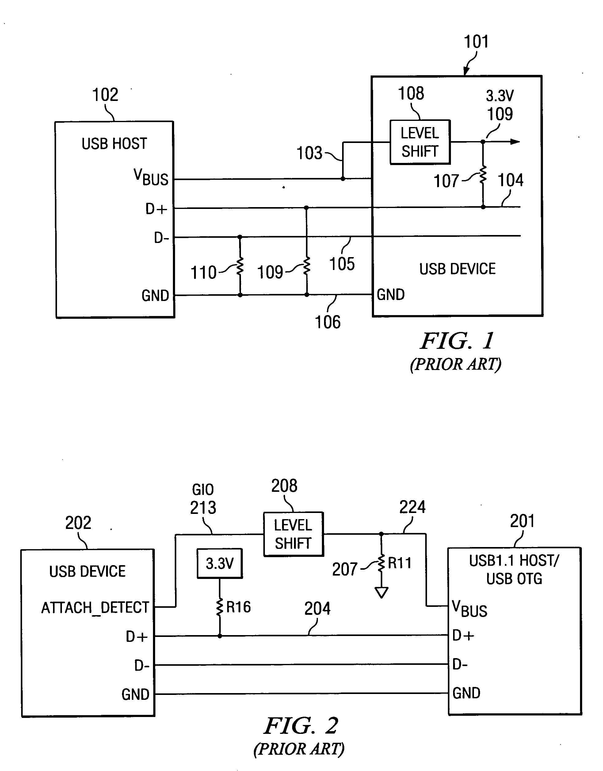
[0018]FIG. 2 illustrates a conventional design for USB attach detection that causes inconsistent attach detection. Level shift device 208 performs 5.0 volts to 3.3 volts voltage conversion. Input voltage Vbus at node 224 is nominally 5.0 volts. The output voltage on 213 (GI0) is 3.3 volts. When the USB device 201 is not attached to the bus, GIO 213 detects low as R11207 pulls the Vbus input 224 to low. When the USB Device 201 is attached to the USB connector, Vbus 224 drives input 213 GIO high to 3.3 volts. In USB suspend mode, an USB 1.1 device connected as block 201 is allowed to draw less than 500 μA from the Vbus 224. The pull down resistor R11207 must therefore be greater than 10.5 KOhms. A non-configured USB OTG device 201 is allowed to draw up to 150 μA from Vbus 224. This requires the pull down resistor 207 (R11) to be greater than 35 KOhms. Assume resistor 207 is 40 KOhms. Then a typical leakage current of 150 μA will set the input level at node 224 to a marginal logic high...
PUM
 Abstract
Description
Claims
Application Information


