

Wafer detecting device
a detection device and glass wafer technology, applied in the field of front-opening interface mechanical standard (fims) system, can solve the problems of large process problem, damage to the wafer, and difficulty in detecting the presence of glass wafers
- Summary
- Abstract
- Description
- Claims
- Application Information
AI Technical Summary
Benefits of technology
Problems solved by technology
Method used
Image

Examples
Embodiment Construction
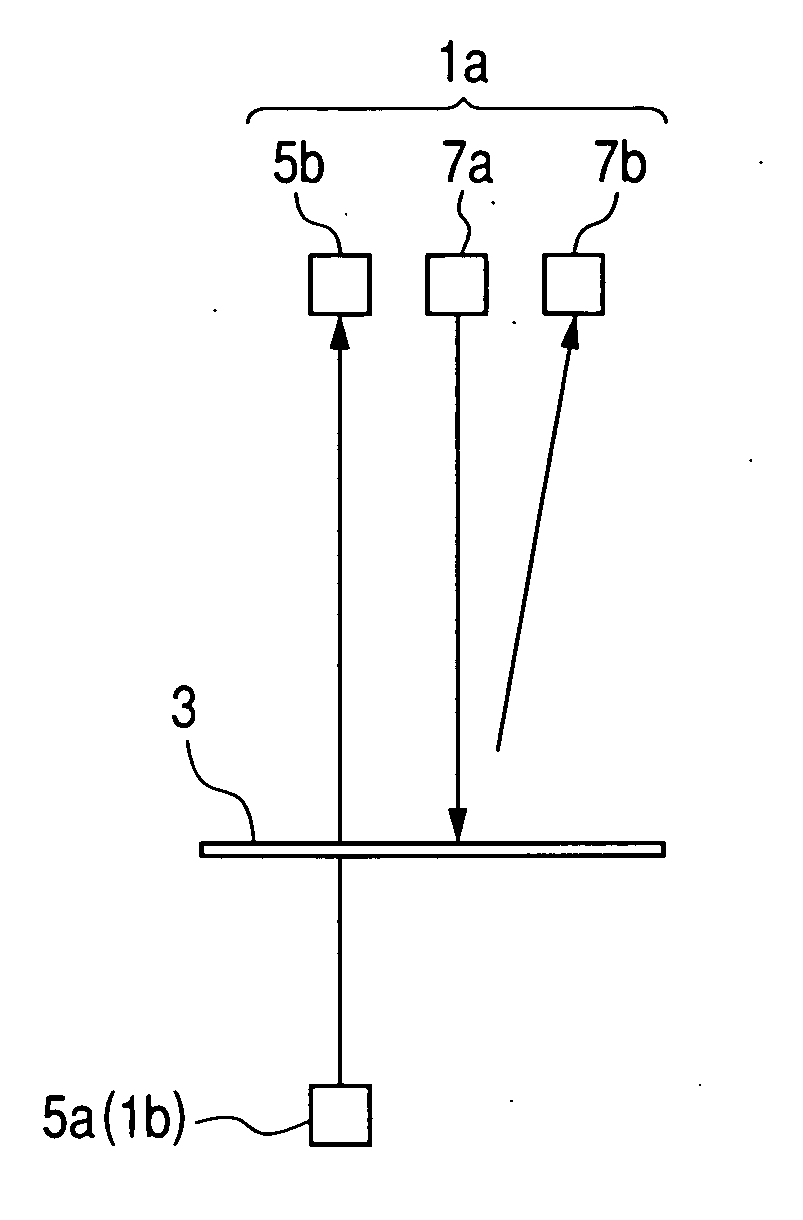
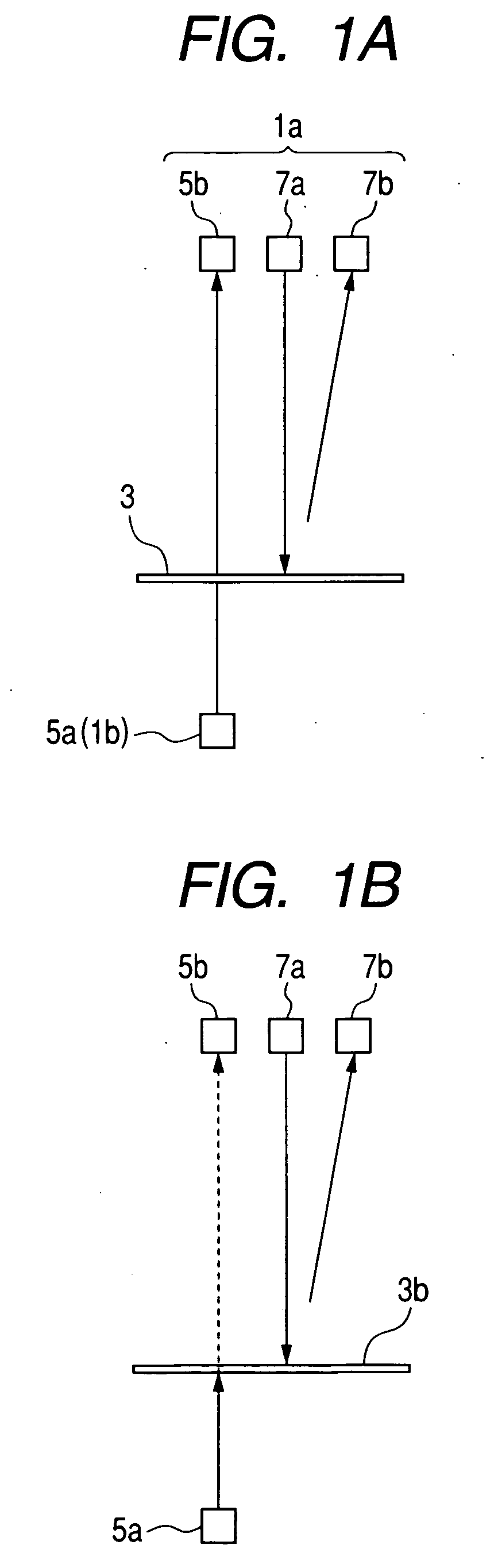
[0021] Hereinafter, a best mode for embodying the present invention will be described with reference to the drawings. FIGS. 1A and 1B are schematic views showing a main structure of the present invention and a principle thereof. A detecting device according to an embodiment of the present invention includes a light transmission sensor having a light emitting portion 5a and a light receiving portion 5b and a light reflection sensor having a light emitting portion 7a and a light receiving portion 7b. That is, according to a structure in the present invention, the light emitting portion of the light reflection sensor, the light receiving portion thereof, and one of the light emitting portion of the light transmission sensor and the light receiving portion thereof are disposed on one surface side of a substrate to be detected (the same surface side as a processed surface of the substrate or a surface side different therefrom) in a position in which the substrate is located (slip-out pos...
PUM
 Abstract
Description
Claims
Application Information