Eureka AIR delivers breakthrough ideas for toughest innovation challenges, trusted by R&D personnel around the world.

Flat display device and method for making the same

a display device and flat display technology, applied in the field of flat display devices, can solve the problems of display damage under and due to atmospheric pressure, display brightness and size increase, and still has problems to be solved concerning a higher brightness and an increase in siz

Inactive Publication Date: 2006-05-04
SONY CORP
View PDF8 Cites 45 Cited by
  • Summary
  • Abstract
  • Description
  • Claims
  • Application Information

AI Technical Summary

Benefits of technology

[0024] The flat-type display of the present invention may have a constitution in which a plurality of spacer holders for temporarily holding the spacer are formed in the first panel effective field and / or the second panel effective field. The above constitution will be referred to as “flat-type display according to the second constitution” for convenience. It is required to arrange the spacer on the first panel effective field and / or the second panel effective field before the spacer is fixed to the first panel effective field and / or the second panel effective field. When the above spacer holders are provided, the falling or tilting of the spacer can be reliably prevented in a step following the arrangement (temporarily holding) of the spacer on the first panel effective field and / or the second panel effective field. A more specific layout, etc., of the spacer holders will be described later.
[0099] In the present invention, since the spacer is fixed to the first panel effective field and / or the second panel effective field with the low-melting-point metal material layer, the tilting or falling of the spacer in the process of producing a flat-type display can be reliably prevented, and the present invention is free from the problems wherein a gas is released from a material fixing the spacer in various heat-treatment steps in the process of producing a flat-type display and wherein the material fixing the spacer is thermally deteriorated.

Problems solved by technology

For applying the liquid crystal display to a floor-type television receiver, however, it still has problems to be solved concerning a higher brightness and an increase in size.
When the spacer 331 is not provided between the anode panel AP and the cathode panel CP, therefore, the display is damaged under and due to atmospheric pressure.
Particularly, when the display is increased in size, the number of the spacers increases, and it is more difficult to hold the spacers perpendicularly.
However, there are remaining problems on the release of a gas from the adhesive and thermal deterioration of the adhesive.
When some gas is present inside the image display, for example, a cold cathode field emission display has problem that since fine electron emitting portions are sputtered with ions generated by the gas, the electron emission efficiency is changed, or that since electron emitting portions are damaged, the lifetime of the image display is decreased.
In the display disclosed in JP-A-10-199451, there is caused a problem wherein because the process for producing an integrated structure of a panel body and a spacer portion is difficult, the production cost is increased.

Method used


Image

  • Flat display device and method for making the same
  • Flat display device and method for making the same
  • Flat display device and method for making the same

Examples


example 1

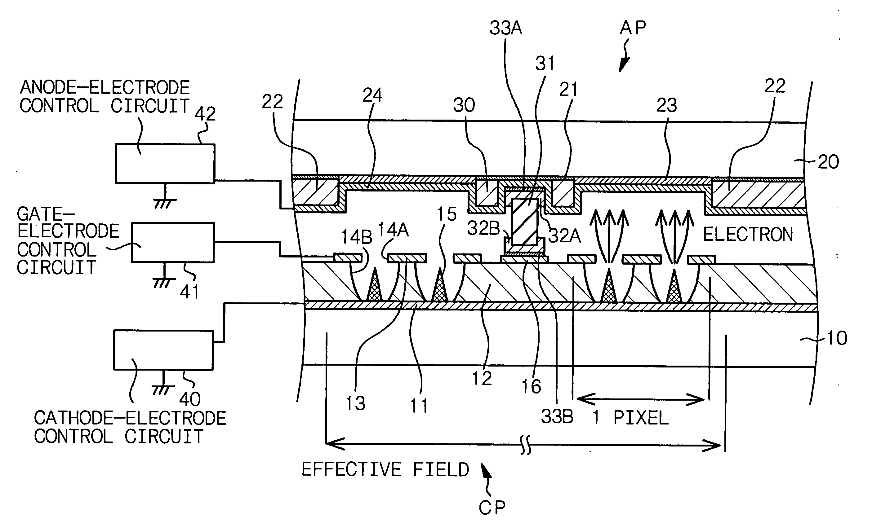
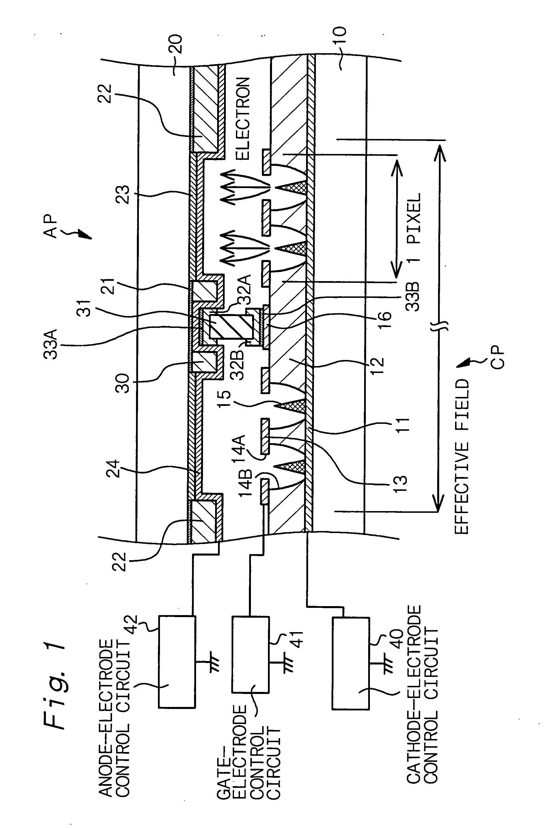
[0123] Example 1 is directed to the flat-type display of the present invention, and more specifically, to the flat-type display according to the first-C aspect (“case 22” in Table 1). Further, it is directed to the method for manufacturing a flat-type display, provided according to the first aspect of the present invention, and more specifically, to the method for manufacturing a flat-type display, provided according to each of the first-A and first-B aspects of the present invention (“case 42” in Table 2). In Example 1, the flat-type display is a cold cathode field emission display (to be simply abbreviated as “display” hereinafter).

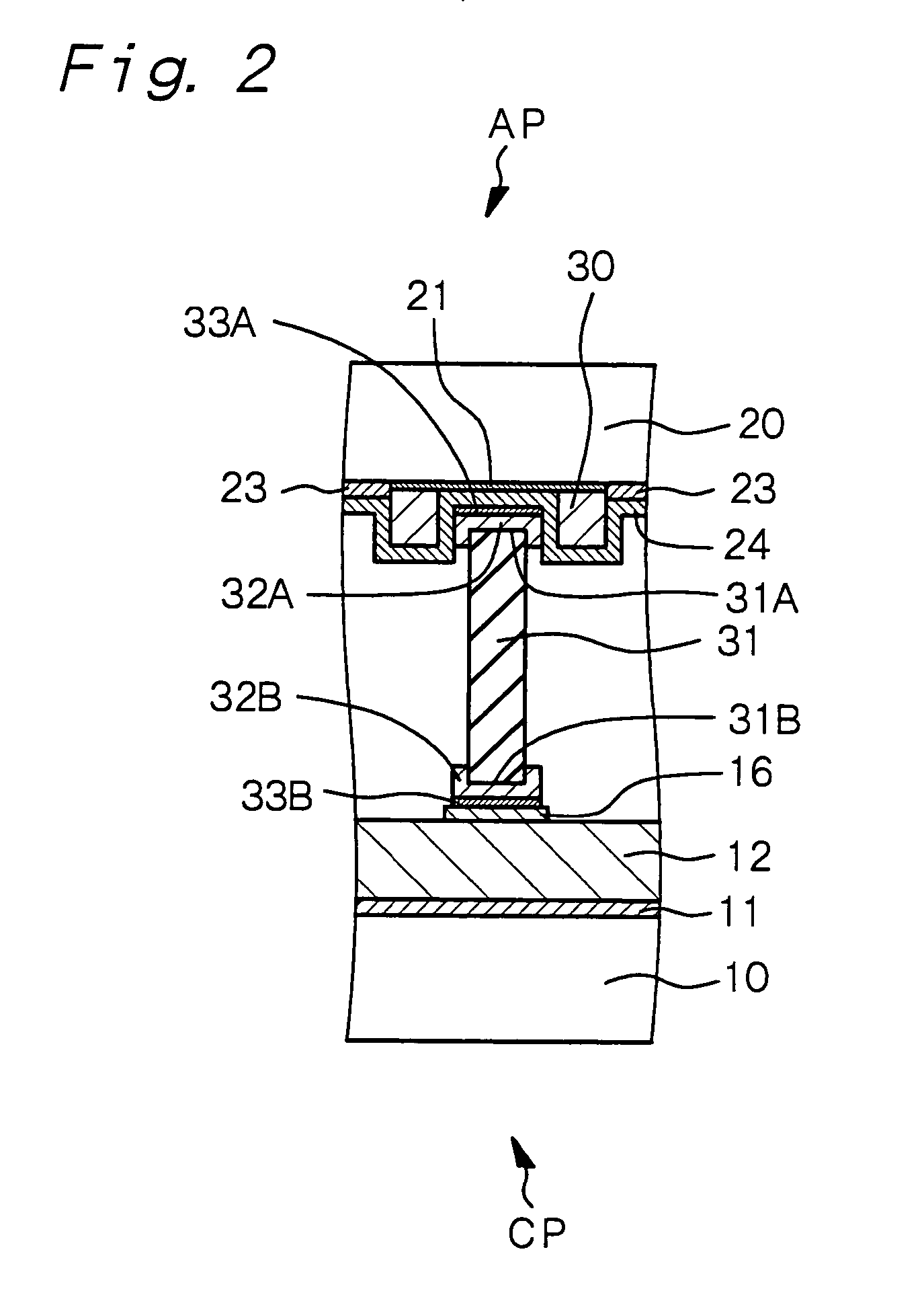
[0124]FIG. 1 shows a schematic partial end view of the display (so-called three-electrode type display) of Example 1, FIG. 2 shows an enlarged schematic end view of part of the display, FIGS. 3 to 5 show layout drawings schematically showing layouts of partition walls 22 and phosphor layers 23 in an anode panel AP constituting the display, and FIG. 6 s...

example 2

[0154] Example 2 is a variant of Example 1 and corresponds to “Case 22” in Table 1 and “Case 42” in Table 2 like Example 1. In Example 2, the spacer holders 30A for temporarily holding the spacer are formed on the cathode panel side. That is, the first panel is a cathode panel CP having a plurality of field emission devices formed thereon, and the second panel is an anode panel AP having the anode electrode 24 and the phosphor layer 23 formed thereon. FIG. 9 shows a schematic partial end view of a display having the above constitution in Example 2, and FIG. 10 shows an enlarged schematic end view of part of the display. FIG. 9 corresponds to an end view taken along arrows A-A in FIG. 3.

[0155] The cathode panel CP having the above structure can be manufactured by the following method.

[0156] That is, the field emission devices are formed on a supporting member 10 corresponding to the substratum. The method for manufacturing the field emission devices will be described in detail late...

example 3

[0164] Example 3 is also a variant of Example 1, and more specifically, it is directed to a flat-type display according to the first constitution (“Case 1” in Table 1) and is also directed to the method for manufacturing a flat-type display, provided according to the first aspect of the present invention (“Case 31” in Table 2).

[0165] In Example 3, a low-melting-point metal material layer 33A is formed on one surface 31A of the spacer 31 which surface is opposed to the first panel (anode panel AP), but no low-melting-point metal material layer 33B is formed on the other surface 31B of the spacer 31 which surface is opposed to the second panel (cathode panel CP). In Example 3, further, neither partition walls nor spacer holders for temporarily holding the spacer are formed in the first panel (anode panel AP). Except for these points, the display in Example 3 can be structured so as to be the same as that of the display in Example 1, so that detailed explanations thereof will be omitt...


PUM


Abstract

A flat-type display comprising a first panel AP and a second panel CP which are bonded to each other in their circumferential portions and having a space between the first panel AP and the second panel CP, the space being in a vacuum state, a spacer being disposed between a first panel effective field and a second panel effective field that work as a display portion, said spacer being fixed to the first panel effective field and / or the second panel effective field with a low-melting-point metal material layers 33A and 33B.

Description

TECHNICAL FIELD [0001] The present invention relates to a flat-type display such as, for example, a cold cathode field emission display, and a manufacturing method thereof. BACKGROUND ART [0002] In the fields of displays for use in television receivers and information terminals, studies have been made for replacing conventionally mainstream cathode ray tubes (CRT) with flat-panel displays which are to comply with demands for a decrease in thickness, a decrease in weight, a larger screen and a high fineness. Such flat panel displays include a liquid crystal display (LCD), an electroluminescence display (ELD), a plasma display panel (PDP) and a cold cathode field emission display (FED). Of these, a liquid crystal display is widely used as a display for an information terminal. For applying the liquid crystal display to a floor-type television receiver, however, it still has problems to be solved concerning a higher brightness and an increase in size. In contrast, a cold cathode field ...

Claims


Application Information

Patent Timeline
Patent Type & Authority Applications(United States)
IPC IPC(8): H01J1/62H01J1/304H01J9/18H01J9/24H01J9/26H01J29/02H01J29/86H01J29/87H01J31/12
CPCH01J9/185H01J9/242H01J29/028H01J29/864H01J31/127H01J2329/8625H01J2329/864H01J2329/8645H01J2329/865H01J2329/8655H01J2329/866H01J2329/8665
Inventor MINAMI, MASARU
Owner SONY CORP
Why Eureka
Eureka Blog
Learn More