CMOS current mirror circuit and reference current/voltage circuit

a current mirror circuit and reference current/voltage circuit technology, applied in the direction of electric variable regulation, process and machine control, instruments, etc., can solve the problems of reference current circuit and difficulty in implementation of current mirror circuit, and achieve the effect of reducing temperature characteristic (dependency) and reducing variation

Inactive Publication Date: 2006-05-04
RENESAS ELECTRONICS CORP
View PDF8 Cites 17 Cited by
  • Summary
  • Abstract
  • Description
  • Claims
  • Application Information

AI Technical Summary

Benefits of technology

[0066] According to the present invention, the circuit is implemented only by the MOS transistors having the same temperature characteristics and the temperature characteristics are mutually cancelled out, thereby reducing the temperature characteristic (dependency).
[0067] According to the present invention, two MOS transistors with gate voltages thereof made common are cascode-connected, for operation in the linear region. The MOS transistor thus can be operated in the linear region with reliability, and the nonlinear current mirror circuit can be configured by using the MOS transistor in place of a resistance element.
[0068] According to the present invention, the MOS transistor is used in place of the resistance element, and no resistance element is employed. A variation thus can be reduced.

Problems solved by technology

In a conventional approach, the reference current circuit has the positive temperature characteristic and it is difficult to implement the current mirror circuit, reference current circuit, and reference voltage circuit all having a small temperature characteristic.

Method used


Image

  • CMOS current mirror circuit and reference current/voltage circuit
  • CMOS current mirror circuit and reference current/voltage circuit
  • CMOS current mirror circuit and reference current/voltage circuit

Examples


Embodiment Construction

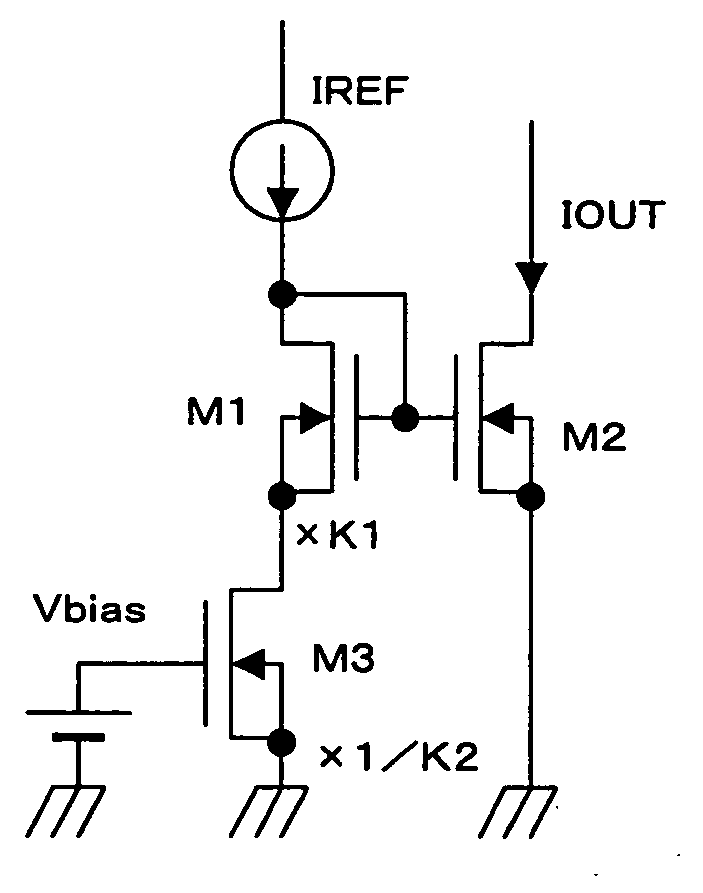
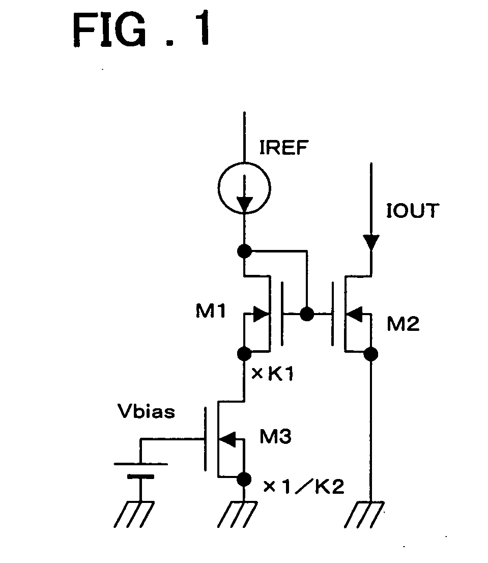
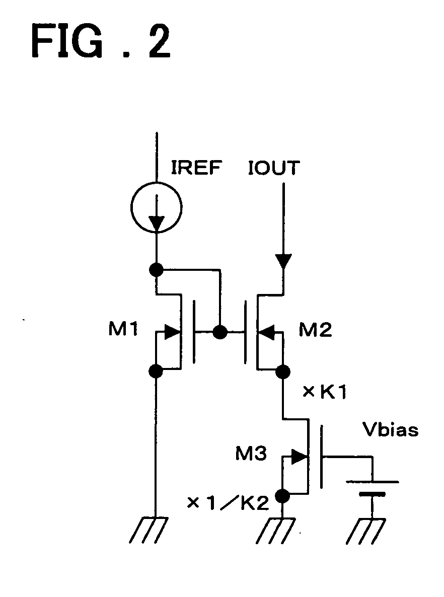
[0093] A best mode for carrying out the present invention will be described. A current mirror circuit according to the present invention includes first and second transistors constituting a current mirror, and includes an active element on the input or output side of the current mirror circuit to accommodate a predetermined nonlinear input-output characteristic of the current mirror circuit. The first transistor and the second transistor are an input side and output side transistors, respectively. Preferably, as the active element, a third transistor with a control terminal thereof being biased to a predetermined potential is connected either of between a ground (power supply) and one terminal of the first transistor (in FIG. 1), between the ground (power supply) and one terminal of the second transistor on the output side (in FIG. 2), or between the first transistor and the supply terminal of an input current (in FIG. 3).

[0094] In a reference current circuit according to the prese...


PUM


Abstract

Disclosed is a CMOS current mirror circuit including a first MOS transistor and a second MOS transistor constituting a current mirror, in which a drain of the first MOS transistor and a gate of the second MOS transistor are connected in common, a source of the first MOS transistor is directly grounded, and a gate of the first MOS transistor is connected to the drain of the first MOS transistor through a third MOS transistor which has a source connected to the drain of the first MOS transistor, a drain connected to the gate of the first MOS transistor, and a gate being biased. The source of the second MOS transistor is directly grounded. Current is input to the drain of the third MOS transistor. The drain current of the second MOS transistor is mirrored by cascode current mirror circuits. An output current is output from the source of a MOS transistor for conversion to a voltage by a circuit that receives the current which outputs a reference voltage.

Description

FIELD OF THE INVENTION [0001] The present invention relates to a CMOS current mirror circuit and a CMOS reference current / voltage circuit. More specifically, the present invention relates to the CMOS current mirror circuit having no resistance element and the CMOS reference current / voltage circuit having a small temperature characteristic, both formed in a semiconductor integrated circuit. BACKGROUND OF THE INVENTION [0002] A nonlinear CMOS current mirror circuit that uses a resistor is described in detail in Patent Document 1 (JP Patent Kokoku Publication No. JP-B-S46-16468), Patent Document 2 (JP Patent No. 2800523), Patent Document 3 (JP Patent No. 3039611), and the like, for example. As the well known CMOS current mirror circuit, a reverse Widlar current mirror circuit shown in FIG. 20 is described in the Patent Document 3 (JP Patent No. 3039611) and the like. [0003] As for a Widlar current mirror circuit shown in FIG. 21, a circuit that uses bipolar transistors is described in ...

Claims


Application Information

Patent Timeline
Patent Type & Authority Applications(United States)
IPC IPC(8): G05F1/10
CPCG05F3/262
Inventor KIMURA, KATSUJI
Owner RENESAS ELECTRONICS CORP
Why Eureka
Try Eureka