Organic thin film transistor and flat panel display including the same

Active Publication Date: 2006-05-18
SAMSUNG DISPLAY CO LTD
View PDF7 Cites 14 Cited by
  • Summary
  • Abstract
  • Description
  • Claims
  • Application Information

AI Technical Summary

Benefits of technology

[0017] The present invention provides an organic thin film transistor having an organic semiconductor layer that does not cause a coffee stain effect and t

Problems solved by technology

However, the manufacturing cost of the conventional silicon thin film transistor having the above-described structure is high, and the conventional silicon thin film transistor is easily broken by an external impact.
In addition, since the silicon thin film transistor is fabricated at a high temperature of 300° C. or more, a plastic substrate cannot be used because it must be treated at low temperature.
However, the plastic substrate must be treated at a low temperature, not the high temperature described above.
Therefore, it is very difficult to use the conventional silicon thin film transistor on plastic substrates.
However, in the organic thin film transistor, it is difficult to pattern the organic semiconductor layer.
In addition, there is a problem with imperfect contact between the organic semiconductor layer and the source and/or drain electrodes.
When patterning the organic semiconductor layer of the organi

Method used


Image

  • Organic thin film transistor and flat panel display including the same
  • Organic thin film transistor and flat panel display including the same
  • Organic thin film transistor and flat panel display including the same

Examples


Embodiment Construction

[0038] Hereinafter, preferred embodiments of the present invention will be described in detail with reference to the accompanying drawings.

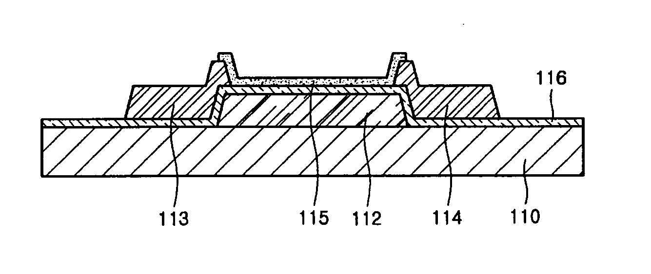
[0039]FIG. 5 is a schematic plan view of an organic thin film transistor according to one embodiment of the present invention. FIG. 6 is a cross-sectional view of an organic thin film transistor taken along line VI-VI of FIG. 5. FIG. 5 does not illustrate a gate electrode, which will be described later.

[0040] Referring to FIGS. 5 and 6, the organic thin film transistor comprises source and drain electrodes 113 and 114, which are isolated from a gate electrode 112, and an organic semiconductor layer 115, which is insulted from the gate electrode 112 but contacts the source and drain electrodes 113 and 114. The organic thin film transistor may further comprise a gate insulating layer 116, which insulates the source and drain electrodes 113 and 114 and the organic semiconductor layer 115 from the gate electrode 112.

[0041] In the structure describ...


PUM


Abstract

An organic thin film transistor comprising an organic semiconductor layer that does not cause a coffee stain effect and can prevent an imperfect contact with source and drain electrodes, and a flat panel display apparatus comprising the organic thin film transistor are provided. The organic thin film transistor comprises a gate electrode; source and drain electrodes insulated from the gate electrode; and an organic semiconductor layer insulated from the gate electrode and contacts the source and drain electrodes, wherein the organic semiconductor layer has a circular shape when viewed through a substrate on which the organic thin film transistor is formed, and an edge portion of at least one of the source and drain electrodes contacting the organic semiconductor layer having a curved shape that is concave toward the organic semiconductor layer.

Description

CROSS-REFERENCE TO RELATED PATENT APPLICATION [0001] This application claims priority to Korean Patent Application No. 10-2004-0094418, filed on Nov. 18, 2004, in the Korean Intellectual Property Office, the disclosure of which is incorporated by reference herein in its entirety. BACKGROUND [0002] 1. Field of the Invention [0003] The present invention relates to an organic thin film transistor and a flat panel display apparatus comprising the organic thin film transistor, and, more particularly, to an organic thin film transistor wherein an organic semiconductor layer does not cause a coffee stain effect and does not have imperfect contact with source and drain electrodes and a flat panel display apparatus comprising the organic thin film transistor. [0004] 2. Discussion of Related Art [0005] Since the development of polyacetylene, a conjugated organic polymer having semiconductor characteristics, organic transistors for functional electronic and optical devices have been widely and...

Claims


Application Information

Patent Timeline
IPC IPC(8): H01L29/08
CPCH01L51/0005H01L51/0021H01L51/0545H10K71/135H10K71/60H10K10/466H10K10/84
Inventor SUH, MIN-CHULKOO, JAE-BON
Owner SAMSUNG DISPLAY CO LTD
Why Eureka
Try Eureka