Printed circuit board and method of manufacturing the same

a printed circuit board and manufacturing method technology, applied in the direction of resistive material coating, electric cable installation, metallic material coating process, etc., can solve the problems of bending of rigid substrate and its core, difference in thermal expansion coefficient between psr ink and core, and the strip process requires higher manufacturing cost than the reel-to-reel process

Inactive Publication Date: 2006-05-18
MDS CO LTD
View PDF24 Cites 29 Cited by
  • Summary
  • Abstract
  • Description
  • Claims
  • Application Information

AI Technical Summary

Benefits of technology

[0021] According to an embodiment of the present invention, there is provided a method of manufacturing a printed circuit board, the method comprising: forming a prepreg layer using a reel method; forming a conductive film; and forming a circuit pattern. More specifically, in an embodiment, the method comprises: forming a prepreg layer which has a thickness of at most about 0.15 mm, and which contains a fiber material and a resin material, the content of the resin material in the prepreg layer is about 70% or less by volume and the prepreg layer is composed of at least one prepreg layer formed via a reel method; forming a conductive film

Problems solved by technology

However, the strip process requires higher manufacturing costs than the reel-to-reel process.
However, when the rigid substrate is manufactured by the reel-to-reel process, bending of the rigid substrate and its core occurs.
The main cause of the bending is the difference in the coefficient of thermal expansion between the PSR ink and the core.
In this case, the bending of the PSR ink cannot be stopped by the core since the core is thin.
The bending of the PSR ink generates cracks between the PSR ink and the core and within the core between the prepreg and the resin material.
That is, since a laser process and a drilling process must be performed, the manufacturing costs of the printed circuit board increase.
However, due to the glass fiber included in the printed circuit board, cracks can be generated

Method used


Image

  • Printed circuit board and method of manufacturing the same
  • Printed circuit board and method of manufacturing the same
  • Printed circuit board and method of manufacturing the same

Examples


Embodiment Construction

[0034] The present invention will now be described more fully with reference to the accompanying drawings in which exemplary embodiments of the invention are shown.

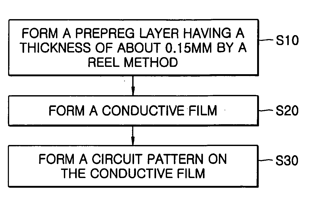
[0035] Referring to FIG. 1, in an embodiment of the present invention, a method of manufacturing a printed circuit board includes: forming a prepreg layer (S10); forming a conductive film on the prepreg layer (S20); and forming a circuit pattern on the conductive film (S30).

[0036] The forming of the prepreg layer (S10) is performed by filling a resin material in a fiber material. In an embodiment, the prepreg layer has a thickness of about 0.15 mm or less. Afterward, to form a circuit pattern on at least one surface of the prepreg layer, an operation for forming the conductive film is performed (S20). In an embodiment, the conductive film is comprised of copper. Next, an operation for forming the circuit pattern is performed through etching the conductive film (S30). Afterward, an operation for forming a protection laye...


PUM

PropertyMeasurementUnit
Lengthaaaaaaaaaa
Fractionaaaaaaaaaa
Fractionaaaaaaaaaa

Abstract

Provided is a method of manufacturing a printed circuit board. In an embodiment, the method includes forming a prepreg layer via a reel method, forming a conductive film for forming a circuit pattern on at least one surface of the prepreg layer; and forming a predetermined circuit pattern on the conductive film. In an embodiment, the prepreg layer has a thickness of at most about 0.15 mm and contains a fiber material and a resin material. In an embodiment, the content of the resin material in the prepreg layer is about 70% or less by volume. In an embodiment, the prepreg layer is composed of at least one prepreg layer.

Description

CROSS-REFERENCE TO RELATED PATENT APPLICATION [0001] This application claims the benefit of Korean Patent Application No. 10-2004-0092269, filed on Nov. 12, 2004, in the Korean Intellectual Property Office, the disclosure of which is incorporated herein in its entirety by reference. BACKGROUND OF THE INVENTION [0002] 1. Field of the Invention [0003] The present invention relates to a printed circuit board and a method of manufacturing the same. More particularly, the present invention relates to a printed circuit board, on which small electronic parts such as chips are mounted, and a method of manufacturing the same. [0004] 2. Description of the Related Art [0005] Small electronic parts, such as semiconductor chips, are generally mounted on a printed circuit board. The printed circuit boards can be divided into flexible substrates and rigid substrates. [0006] The rigid substrate typically consists of a raw material layer, an electro deposit copper (Cu) layer, and photo solder resist...

Claims


Application Information

Patent Timeline
IPC IPC(8): B05D5/12
CPCH05K1/0366H05K3/022Y10S428/901Y10T428/24926Y10T428/24917H05K2203/1545H01L23/538
Inventor JANG, CHANG-SOORYU, JAE-CHULROH, HYOUNG-HOWON, DONG-KWAN
Owner MDS CO LTD
Why Eureka
Try Eureka