Image sensor for still or video photography

a technology of image sensor and still photography, applied in the direction of picture signal generator, television system scanning details, television system, etc., can solve the problems of only 4% of the photodiode used in sub-sampling images, still leaving some pixels un-sampled, and inconvenient, so as to reduce the resolution of the image sensor

Inactive Publication Date: 2006-06-15
SEMICON COMPONENTS IND LLC
View PDF12 Cites 32 Cited by
  • Summary
  • Abstract
  • Description
  • Claims
  • Application Information

AI Technical Summary

Benefits of technology

[0015] The present invention includes the advantage of reducing the image sensor resolution by a factor of 5 while sampling the entire pixel array.

Problems solved by technology

This is not suitable if the same camera is to be used for recording video.
The disadvantage of sub-sampling the image by a factor of 5 is only 4% of the photodiodes are used.
However, this prior art still leaves some pixels un-sampled.
Another disadvantage of the prior art is it only reduces the image resolution in the vertical direction.
However, this prior art requires a striped color filter pattern (a 3×1 color filter array), which is generally acknowledged to be inferior to the Bayer or 2×2 color filter array patterns.

Method used


Image

  • Image sensor for still or video photography
  • Image sensor for still or video photography
  • Image sensor for still or video photography

Examples


first embodiment

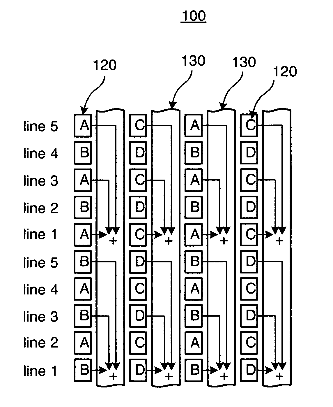
[0051] the sequence of steps to reduce the image sensor 100 resolution by a factor of 5 is shown in FIGS. 6a through 6c. The rows of photodiodes 120 are grouped into five sequentially numbered lines. The first step in FIG. 6a is to simultaneously transfer charge from all of the odd numbered lines from the photodiodes 120 to the VCCD 130. The first set of three lines 1, 3, and 5 transfer colors B and D into the VCCD 130. The next set of three lines 1, 3, and 5 transfers colors A and C into the VCCD 130. If the camera is used outside in bright sunlight, the summing of pixels will enhance the sensitivity such that a very short exposure time will be required. The exposure time might be as short as 100 to 200 μs. If the photodiodes 120 from color A are transferred to the VCCD 130 before photodiodes 120 from color B, the color B photodiodes will receive a longer exposure time than the photodiodes 120 from color A. Thus, video recording with very short exposure times will show an undesirab...

second embodiment

[0057] After the summing process, the charge packets in the VCCD 130 as shown in FIG. 6c are not equally weighted. One charge packet contains charge from 3 photodiodes of color B and another contains charge from 2 photodiodes of color B. An alternate second embodiment of the summing process to obtain charge packets of equally weighted colors is shown in FIGS. 9a, 9b and 9c. In FIG. 9a, lines 1 and 5 are summed together and the line 3 photodiodes 120 are not transferred to the VCCD 130. Next in FIG. 9b, charge from lines 2 and 4 are transferred and summed together in the VCCD 130. The step shown in FIG. 9b may be omitted to reduce the number of lines to read out to the image sensor by half. Skipping the reading out of lines 2 and 4 would cause some loss of resolution and color information but the faster frame rate might be more desirable. The resulting summed charge packets in FIG. 9c are transferred in parallel towards a serial readout CCD register(s). The photodiodes 120 from line ...

third embodiment

[0059] the charge summing process is shown in FIGS. 11a, 11b, and 11c. In FIG. 11a charge from lines 4 and 5 are simultaneously transferred from the photodiodes 120 to the VCCD 130. The charge packets in the VCCD are kept separate to avoid mixing colors. Then the two charge packets are transferred down two lines in the VCCD. This aligns the charge packet that originated from line 5 with the photodiode in line 3. The charge packet that originated from line 4 will be aligned with the photodiode in line 2. Next in FIG. 11b, charge is transferred from the photodiodes in lines 2 and 3 into and on top of the charge packets already in the VCCD. The result is shown in FIG. 11c where there are now two charge separate packets of two colors in each column. The photodiodes in line 1 are never transferred into the VCCD. The charge packets in the VCCD are transferred in parallel towards a serial readout CCD register(s).

[0060]FIG. 12 shows the charge packet clocking details. FIG. 12 is a cross sec...


PUM


Abstract

A method for reading out charge from an interlined CCD having a plurality of photo-sensing regions and a plurality of vertical shift registers, and each photosensitive region is mated respectively to a CCD of a vertical shift register and a color filter having a repeating pattern of two rows in which each row includes at least two colors that forms a plurality of 5 line sub-arrays sequentially numbered in the space domain; and the color filter spanning the photo-sensing regions, the method includes sequentially or substantially simultaneously reading out lines 1, 3 and 5 into the vertical shift register that keeps the colors separated; summing the charge in lines 1, 3 and 5; sequentially or substantially simultaneously reading out lines 2 and 4 into the vertical shift register that keeps the colors separated; summing the charge in lines 2 and 4; transferring one or more rows of the summed charge into a first horizontal charge-coupled device; transferring alternate charges in the first horizontal charge-coupled device into a second horizontal charge-coupled device; summing sets of two charges in the first horizontal charge-coupled device; summing sets of two charges in the second horizontal charge-coupled device; and reading out the charge in both the first and second horizontal shift register with a half-resolution clocking sequence.

Description

FIELD OF THE INVENTION [0001] The invention relates generally to the field of image sensors for still photography and, more particularly, to producing video of five times less vertical resolution from such image sensors typically used for still photography by sampling the entire array of the image sensor and summing all pixel values in a predetermined manner. BACKGROUND OF THE INVENTION [0002] Referring to FIG. 1, an interline charge coupled device (CCD) image sensor 10 is comprised of an array of photodiodes 20. The photodiodes are covered by color filters to allow only a narrow band of light wavelengths to generate charge in the photodiodes. Typically image sensors have a filter with a pattern of three or more different colors arranged spanning over the photodiodes in a 2×2 sub array as shown in FIG. 2. For the purpose of a generalized discussion, the 2×2 array is assumed to have four colors, A, B, C, and D. The most common color filter pattern used in digital cameras is often ref...

Claims


Application Information

Patent Timeline
Patent Type & Authority Applications(United States)
IPC IPC(8): H04N5/335H04N5/345H04N5/347H04N5/3728H04N5/376H04N9/07
CPCH04N3/1562H04N9/045H04N25/445H04N25/46H04N25/70H04N25/73H04N25/447
Inventor PARKS, CHRISTOPHER
Owner SEMICON COMPONENTS IND LLC
Why Eureka
Try Eureka