Multiple layer structure for substrate noise isolation

a multi-layer structure and substrate technology, applied in the direction of semiconductor devices, semiconductor/solid-state device details, electrical devices, etc., can solve the problems of digital circuit noise interference with the proper functioning of analog circuits, and achieve high impedance noise, high impedance noise, and high impedance noise.

Active Publication Date: 2006-07-27
GLOBALFOUNDRIES U S INC
View PDF32 Cites 14 Cited by
  • Summary
  • Abstract
  • Description
  • Claims
  • Application Information

AI Technical Summary

Problems solved by technology

Noise generated by the digital circuits interferes with the proper functioning of the analog circuits.

Method used


Image

  • Multiple layer structure for substrate noise isolation
  • Multiple layer structure for substrate noise isolation
  • Multiple layer structure for substrate noise isolation

Examples


second embodiment

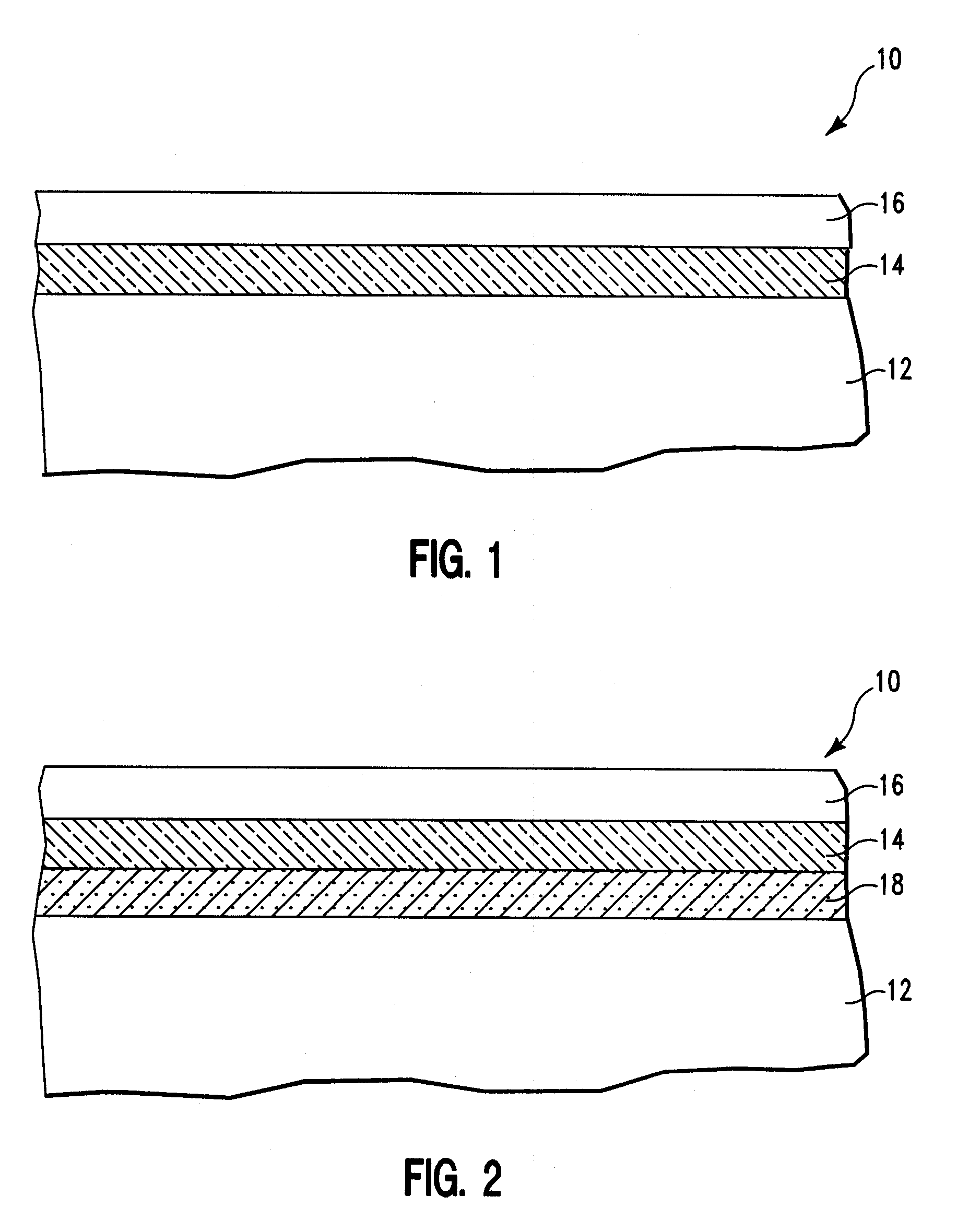
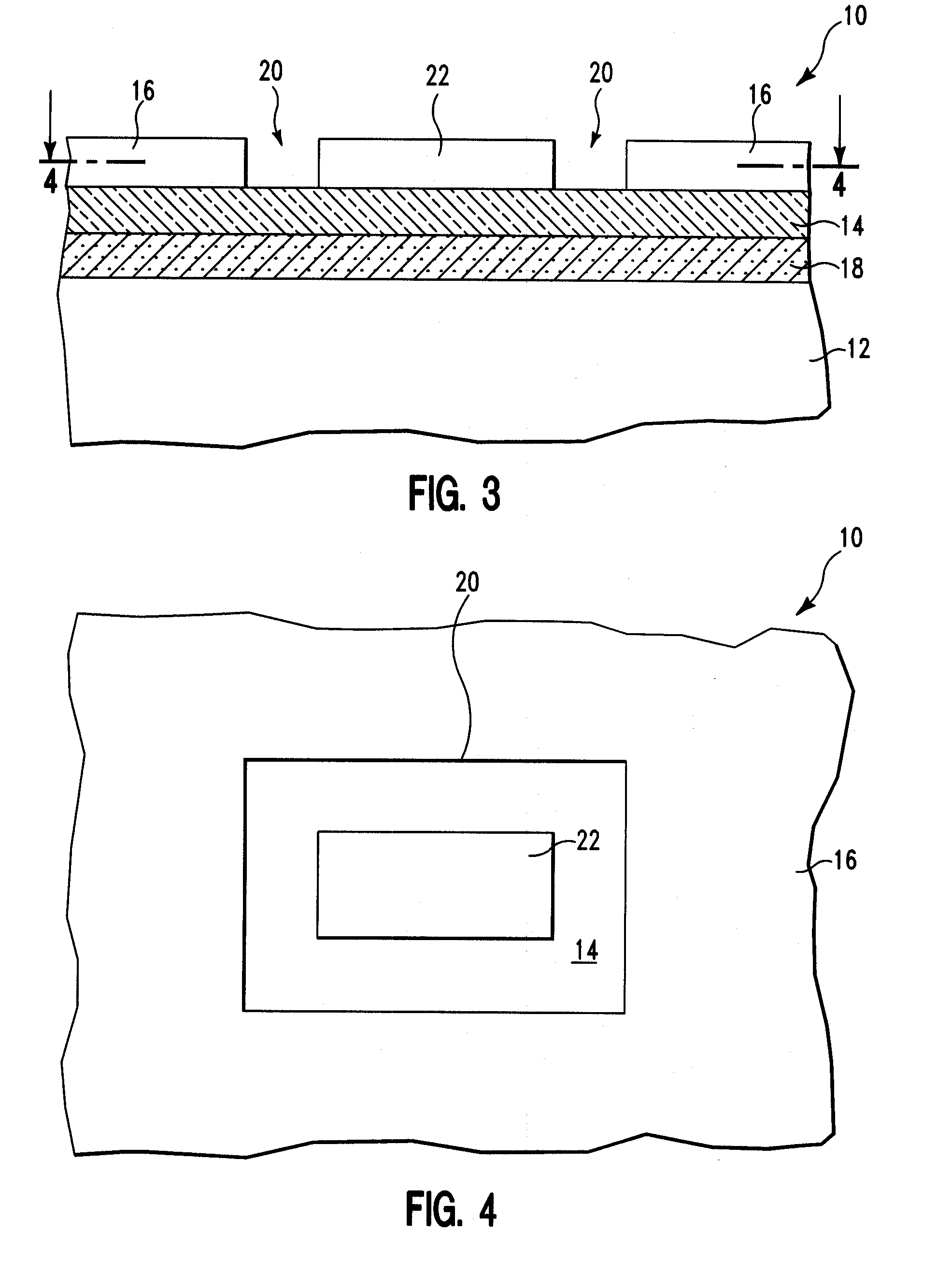
[0055] In accordance with a second embodiment, an SOI 100 comprising a semi-conductive substrate 112, such as silicon (p− or n−), a buried oxide layer 114, such as silicon dioxide, and an upper semi-conductive layer 116 above the buried oxide layer 114, that may comprise the same, or a similar, material as the substrate 112, is formed (FIG. 9). Following formation of the SOI 100, a first heavily doped layer 118 is formed within the SOI 100, beneath the buried oxide layer 114, as illustrated in FIG. 10. The first heavily doped layer 118 may comprise a p+ silicon doped with B, or other similarly used material. The first heavily doped layer 118 may be formed by a conventional ion implantation process, etc. The first heavily doped layer 118 may be formed having a thickness in the range of about 10-500 nm.

[0056] Also illustrated in FIG. 10, a second heavily doped layer 120 is formed within the SOI 100, beneath the buried oxide layer 114 and above the first heavily doped layer 118. The se...

third embodiment

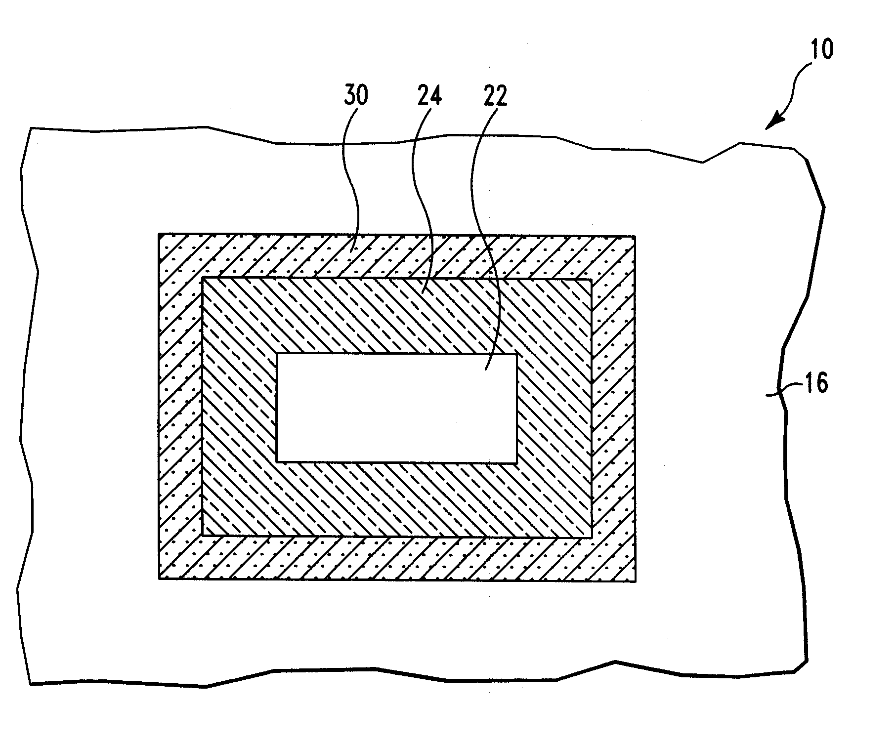
[0065] In accordance with the present invention, an SOI 200 comprising an semi-conductive substrate 212, such as silicon (p− or n−), a first buried oxide layer 214, such as silicon dioxide, a second buried oxide layer 216, such as silicon dioxide, and an upper semi-conductive layer 218 above the second buried oxide layer 216, that may comprise the same material as the substrate 212, are formed (FIG. 26). A heavily doped layer 220 is then formed between the first isolation layer 214 and the second buried oxide layer 216. The heavily doped layer 220 may comprise silicon (p+ or n+) doped with As, P, B, or other similarly used material. One method of forming the SOI structure 200 is to implant oxygen ions twice, each time with different implant energies. The higher energy oxygen ions are implanted within the deeper, or second buried oxide, layer 216 and the lower energy oxygen ions are implanted within the shallower, or first buried oxide, layer 214. Arsenic, P, B, or other similarly us...


PUM


Abstract

A method of forming a semiconductor structure, comprising: providing a substrate having a buried insulative layer and a heavily doped layer; forming a first trench within the substrate around a protected area; filling the first trench with an insulative material, wherein the first trench filled with the insulative material and the buried insulative layer combine to form a high impedance noise isolation that surrounds the protected area on all sides except one side of the protected area to isolate noise from the protected area; forming a second trench within the substrate around the first trench; and filling the second trench with a conductive material, wherein the second trench filled with the conductive material and the heavily doped layer combine to form a low impedance ground path that surrounds the high impedance noise isolation on all sides except one side of the high impedance noise isolation to isolate noise from the protected area.

Description

BACKGROUND OF THE INVENTION [0001] 1. Technical Field [0002] The present invention relates generally to semiconductor structures, and more particularly, to a method of forming a structure for noise isolation, and the structure so formed. [0003] 2. Related Art [0004] Within electrical devices there are device elements that generate noise, such as digital circuits, and others that are noise sensitive, such as analog circuits. Noise generated by the digital circuits interferes with the proper functioning of the analog circuits. [0005] Therefore, there is a need in the industry for a method of forming semiconductor structures that can isolate or filter out the noise, generated by the digital circuits, from reaching and disrupting the more sensitive analog circuits. SUMMARY OF THE INVENTION [0006] The present invention provides a method of forming semiconductor structures, and the structures so formed, that solve the above-stated and other problems. [0007] A first aspect of the invention...

Claims


Application Information

Patent Timeline
Patent Type & Authority Applications(United States)
IPC IPC(8): H01L21/76H01L29/00H01L23/58H01L23/552
CPCH01L21/76264H01L23/552H01L23/585H01L2924/3011H01L2924/0002H01L2924/00
Inventor DING, HANYIFENG, KAI D.HE, ZHONG-XIANGLIU, XUEFENG
Owner GLOBALFOUNDRIES U S INC
Why Eureka
Try Eureka