Back-illuminated imaging device and method of fabricating same

a back-illuminated, imaging device technology, applied in the direction of semiconductor devices, solid-state devices, radio-controlled devices, etc., can solve the problems of reducing the overall efficiency and sensitivity of the device, adding to the complexity of the fabrication process, and methods that cannot be easily included in conventional semiconductor foundry processing, so as to effectively eliminate the dead band on the backsid

Active Publication Date: 2006-08-24
SRI INTERNATIONAL
View PDF4 Cites 73 Cited by
  • Summary
  • Abstract
  • Description
  • Claims
  • Application Information

AI Technical Summary

Benefits of technology

[0008] A goal of inventive process is to create a desired dopant profile and a resulting electric field within a sufficiently thin semiconductor layer. The layer will include the region within which the radiation being detected is absorbed. Another goal of inventive process is to effectively eliminate a backside dead band by creating a desired dopant gradient within a sufficiently thin semiconductor layer.

Problems solved by technology

It is also desirable to minimize the recombination of the generated carriers before they reach the front side, since such recombination reduces overall efficiency and sensitivity of the device.
This requires additional treatment at the backside of the device, which adds to complexity of the fabrication process.
These methods can not be easily included in conventional semiconductor foundry processing, and require more expensive custom processing.
They are therefore often not cost-effective and not suitable for commercial manufacturing.
For silicon imaging devices designed to operate in the deep ultraviolet (UV) wavelength range, the problem of getting the majority of generated carriers from the backside to the front side may be especially challenging, since the radiation is absorbed, and the carriers generated, within about 20 nanometers (nm) of the back surface.
Since, in silicon, most of the UV radiation is absorbed within the same approximately 20 nm region near the back surface, most of the generated electrons may be trapped in this dead band, resulting in poor sensitivity.

Method used


Image

  • Back-illuminated imaging device and method of fabricating same
  • Back-illuminated imaging device and method of fabricating same
  • Back-illuminated imaging device and method of fabricating same

Examples


Embodiment Construction

[0015] The following embodiments are intended as exemplary, and not limiting. In keeping with common practice, figures are not necessarily drawn to scale.

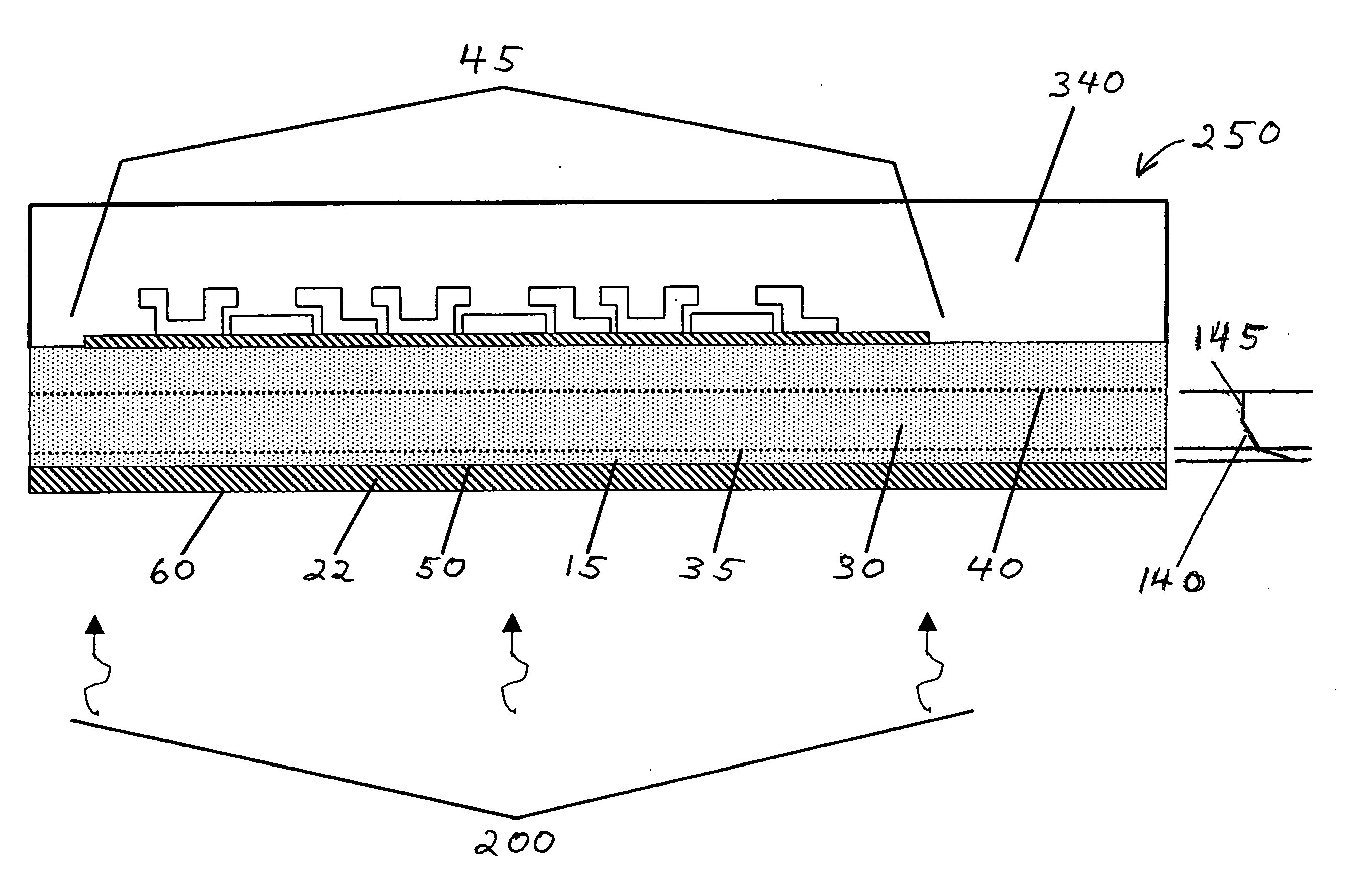
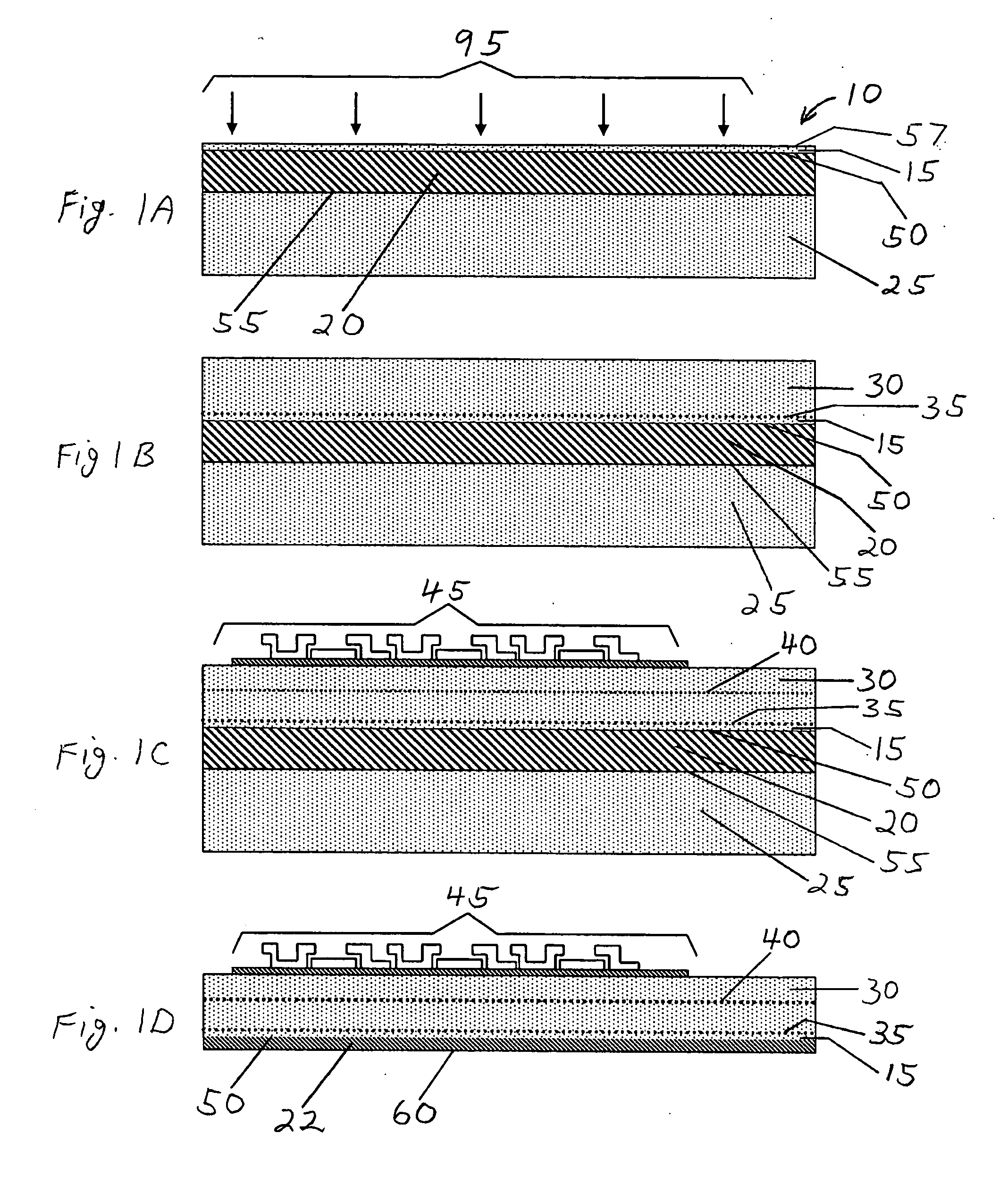
[0016]FIGS. 1A, 1B, 1C, and 1D illustrate an embodiment of a process and a resulting structure. FIG. 1A illustrates initial substrate 10 sometimes referred to in the art as an ultra-thin semiconductor-on-insulator (UTSOI) substrate. FIG. 1B illustrates the state of process embodiment following growth of epitaxial layer 30. FIG. 1C illustrates the state of process embodiment following a step of fabrication of imaging components 45 on and in epitaxial layer 30. As part of this step, one or more electrical junctions, or “pn-junctions”40 are formed in epitaxial layer 30. FIG. 1D illustrates a completed state of the process and the resulting imaging device. Details of each step follow.

[0017] Starting UTSOI substrate 10, shown in FIG. 1A, is composed of mechanical substrate 25 to provide mechanical support during processing, insulator ...


PUM


Abstract

A method for fabricating a back-illuminated semiconductor imaging device on a thin semiconductor-on-insulator substrate, and resulting imaging device. Resulting device has a monotonically varying doping profile which provides a desired electric field and eliminates a dead band proximate to the backside surface.

Description

FIELD OF THE INVENTION [0001] The field of invention is semiconductor device fabrication and device structure. More specifically, the field is fabrication and structure of back-illuminated semiconductor imaging devices. BACKGROUND OF THE INVENTION [0002] Thinned, back illuminated, semiconductor imaging devices are advantageous over front-illuminated imagers for high fill factor and better overall efficiency of charge carrier generation and collection. A desire for such devices is that the charge carriers generated by light or other emanation incident on the backside should be driven to the front side quickly to avoid any horizontal drift, which may smear the image. It is also desirable to minimize the recombination of the generated carriers before they reach the front side, since such recombination reduces overall efficiency and sensitivity of the device. [0003] These desires may be achieved by providing a thin semiconductor layer and a high electric field within this layer. The fie...

Claims


Application Information

Patent Timeline
Patent Type & Authority Applications(United States)
IPC IPC(8): H01L31/00H01L21/00
CPCH01L27/14643H01L27/148H01L27/1464H01L31/1892Y02E10/50H01L31/18
Inventor SWAIN, PRADYUMNABHASKARAN, MAHALINGAM
Owner SRI INTERNATIONAL
Why Eureka
Try Eureka