Liquid Crystal Display Device

a display device and liquid crystal technology, applied in semiconductor devices, optics, instruments, etc., can solve the problems of low power consumption, display is not viewed so well, and the power consumption of a transmission type display device is inconsiderable, so as to improve productivity, enhance the scattering ability of light and hence display visibility, and reduce cost

Active Publication Date: 2006-09-07
SEMICON ENERGY LAB CO LTD
View PDF87 Cites 10 Cited by
  • Summary
  • Abstract
  • Description
  • Claims
  • Application Information

AI Technical Summary

Benefits of technology

[0016] In order to solve the foregoing problem, the present invention is characterized in that, in manufacturing a transflective liquid crystal display device, a reflection electrode of a plurality of irregularly arranged island-like patterns and a transparent electrode of transparent conductive film are layered in forming an electrode having transparent and reflection electrodes thereby providing a concavo-convex form and enhancing the scattering ability of light and hence display visibility. Furthermore, because the plurality of irregularly arranged island-like patterns can be formed simultaneous with the interconnection, a concavo-convex structure can be formed in the manufacturing process without especially increasing the patterning process only for forming a concavo-convex structure. Accordingly, it is possible to greatly reduce cost and improve productivity.
[0023] Incidentally, according to each of the above structures, it is possible to form, by etching, the plurality of irregularly arranged island-like patterns of a reflective conductive film and the interconnection. Furthermore, in the case of simultaneously forming them by etching, because a concavo-convex structure can be configured as viewed at a film-forming surface of the reflective conductive film, it is possible to reduce the photolithography process used in usually forming a concavo-convex structure. This can realize great cost reduction and improvement in productivity.
[0024] Meanwhile, the plurality of irregularly arranged island-like patterns to be formed in each of the above structures are formed and arranged in a random form, and electrically connected to the first transparent conductive film. However, the island-like pattern formed by etching the reflective conductive film is desirably given a smaller taper angle at a pattern end in view of improving the ability of reflection. Incidentally, the plurality of island-like patterns of the invention is characterized by a taper angle of 5-60 degrees at each pattern end.

Problems solved by technology

Power consumption of a transmission type display device is inconsiderable for driving only a display.
For use of a cellular phone, an EL back light is generally used, however, power is additionally needed for the back light and a specific characteristic of low power consumption of a liquid crystal is not fully utilized, which are disadvantageous in low power consumption.
Further, although in a dark environment, display of a display is viewed with excellent contrast, in an ordinary bright environment, the display is not viewed so well and there is a drawback in adaptability in accordance with the environment of use both in cases of an upper emitting type and a lower emitting type.
However, similar to the case of the transmission type liquid crystal display device, although in a dark environment, display of a display is viewed excellently, in an ordinary bright environment, the display is not viewed so well and therefore, there is still a drawback in adaptability in accordance with an environment of use both in cases of the upper emitting type and the lower emitting type.
Further, quite contrary to the former two, although in a bright environment, display of a display is viewed excellently, in a dark environment, the display is not viewed so well.
Considering the use of a portable information terminal, the portable information terminal is mainly used outdoors and there is frequently a case of viewing the display in a comparatively bright environment, however, this is still insufficient in terms of adaptability in accordance with an environment of use.
If a display is fabricated under such a state, a display having very poor visibility is brought about.
The increase of processes would incur a disadvantageous situation, including yield reduction, prolonged process time and increasing cost.

Method used


Image

  • Liquid Crystal Display Device
  • Liquid Crystal Display Device
  • Liquid Crystal Display Device

Examples


example 1

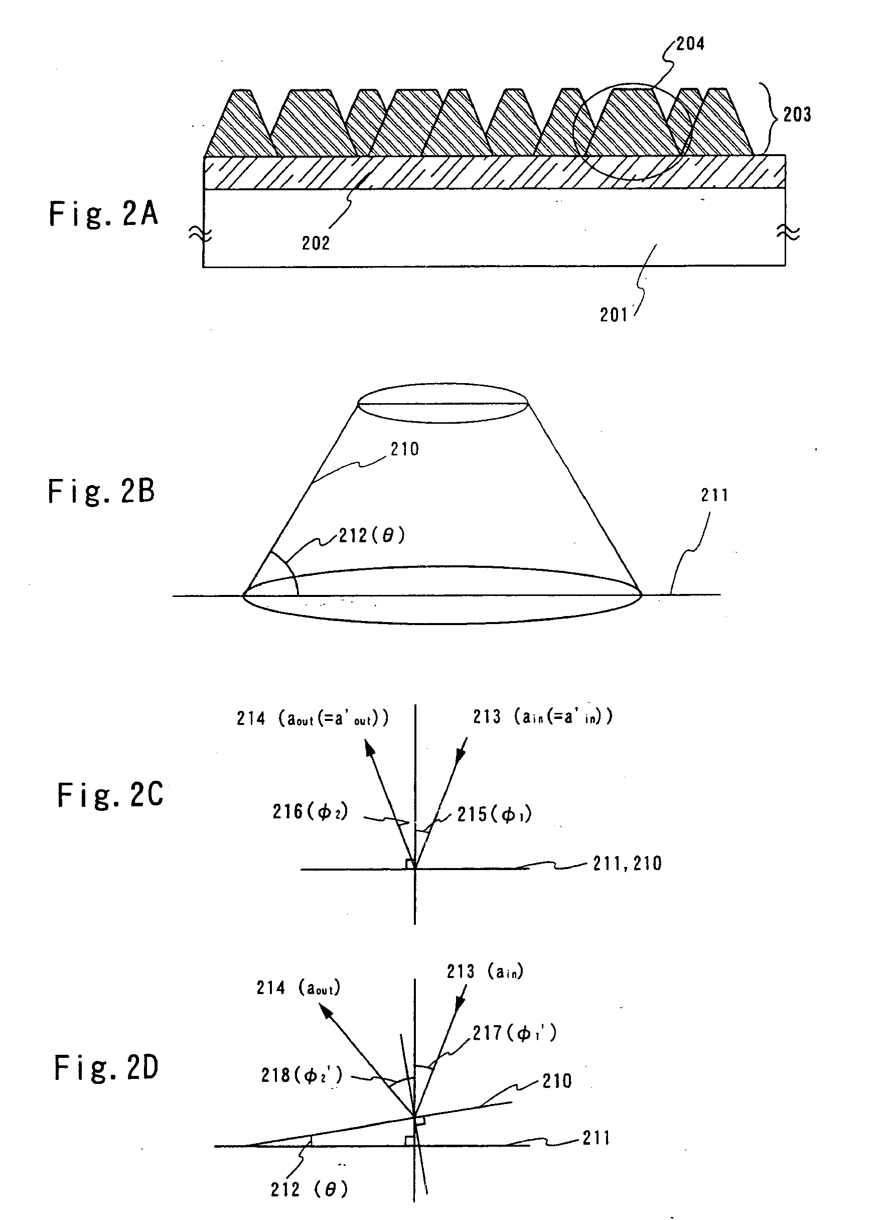
[0061] According to the example, an example of steps of fabricating an active matrix substrate having a top gate type TFT will be shown. Further, FIG. 3A through FIG. 7 showing top views and sectional views of a portion of a pixel portion will be used for explanation.

[0062] First, an amorphous semiconductor layer is formed over a substrate 301 having an insulating surface. Here, a quartz substrate is used as the substrate 301 and the amorphous semiconductor layer is formed with a thickness of 10 through 100 nm.

[0063] Further, a glass substrate or a plastic substrate can be used other than the quartz substrate. When the glass substrate is used, the glass substrate may be subjected to a heat treatment previously at a temperature lower than a glass strain point by about 10 through 20° C. Further, a base film comprising an insulating film such as a silicon oxide film, a silicon nitride film, a silicon oxynitride film and the like may be formed on a surface of the substrate 301 for for...

example 2

[0091] This example concretely explains a method for manufacturing a transflective type liquid crystal display device different in structure from Example 1.

[0092] At first, an amorphous semiconductor film is formed over a substrate 801 as shown in FIG. 8A. After crystallizing this, a semiconductor layer 805 is formed which is separated in an island form by patterning. Furthermore, on the semiconductor layer 805, a gate insulating film 806 is formed by an insulating film. Incidentally, the manufacturing method of up to forming a gate insulating film 806 is similar to that shown in Example 1, and hence reference may be made to Example 1. Similarly, after forming an insulating film coverings the semiconductor layer 805, thermal oxidation is carried out to form a gate insulating film 806.

[0093] Then, a channel dope process is carried out over the entire surface or selectively, to add a p-type or n-type impurity element at low concentration to a region to be made into a TFT channel reg...

example 3

[0113] This example explains a method for manufacturing an active matrix substrate different in structure from the one showing in Examples 1 and 2.

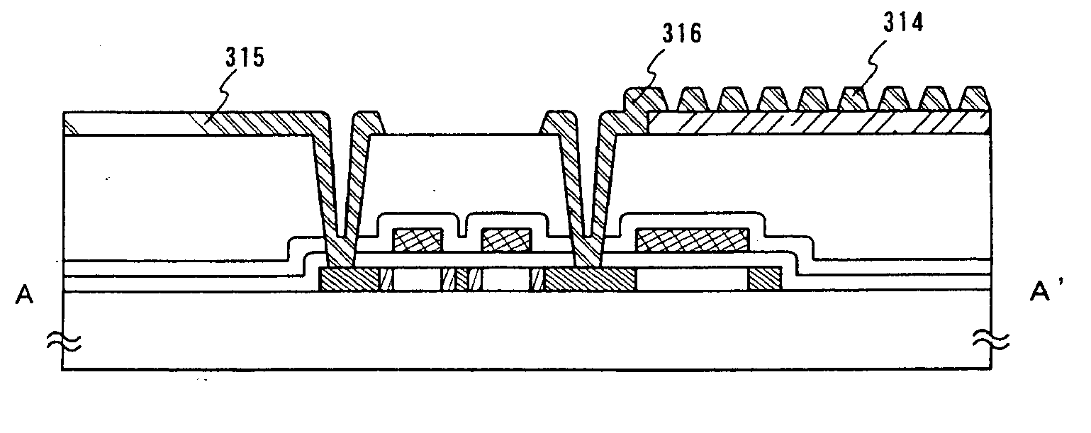
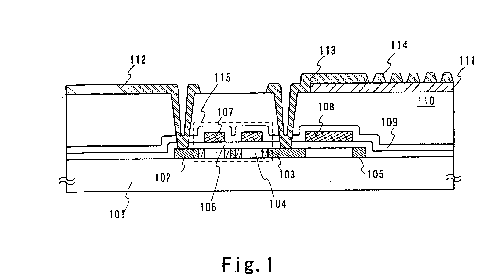
[0114] In FIG. 12, over a substrate 1201 is formed a TFT 1215 having a gate electrode 1207, a source region 1202, a drain region 1203 and interconnections 1212 and 1213. The interconnections 1212 and 1213 are respectively, electrically connected to the source region and the drain region.

[0115] Incidentally, the active matrix substrate of this example is different from Examples 1 and 2 in that a transparent electrode 1211 is formed after forming the interconnections 1212 and 1213.

[0116] Similarly to the one showing in Example 1 or 2, a second insulating film 1210 is formed and, after a contact hole is formed therein, a second conductive film is formed. The material of the second conductive film used herein can use the same material as that of Example 1 or 2.

[0117] By patterning the second conductive film, it is possible to form interco...


PUM

PropertyMeasurementUnit
taper angleaaaaaaaaaa
reflectivityaaaaaaaaaa
thicknessaaaaaaaaaa

Abstract

It is an object to provide a display having high visibility and a transflective type liquid crystal display device having a reflection electrode having a concavo-convex structure formed without especially increasing the process. During manufacturing a transflective liquid crystal display device, a reflection electrode of a plurality of irregularly arranged island-like patterns and a transparent electrode of a transparent conductive film are layered in forming an electrode having transparent and reflection electrodes thereby having a concavo-convex form to enhance the scattering ability of light and hence the visibility of display. Furthermore, because the plurality of irregularly arranged island-like patterns can be formed simultaneous with an interconnection, a concavo-convex structure can be formed during the manufacturing process without especially increasing the patterning process only for forming a concavo-convex structure. It is accordingly possible to greatly reduce cost and improve productivity.

Description

BACKGROUND OF THE INVENTION [0001] 1. Field of the Invention [0002] The present invention relates to a liquid crystal display device of a passive matrix type and an active matrix type. Particularly, the invention relates to an electrode structure of a transflective type liquid crystal display device having both functions of a transmission type and a reflection type. [0003] 2. Description of the Related Art [0004] In recent years, by explosive spread of a portable information terminal represented by a cellular phone, there is needed a display capable of dealing with light-weighted formation, low power consumption and a change in an environment of use. [0005] Further, in views of thin film formation and light-weighted formation, a liquid crystal display device or an organic EL display device is representatively promising. [0006] Power consumption of a transmission type display device is inconsiderable for driving only a display. However, a liquid crystal per se does not emit light and...

Claims


Application Information

Patent Timeline
Patent Type & Authority Applications(United States)
IPC IPC(8): G02F1/136G02F1/1335G02F1/1343H01L21/3205H01L21/336H01L29/786
CPCG02F1/133555G02F1/1335G02F1/134309G02F1/13439G02F1/136227G02F1/1368G02F2201/123H01L27/1255H01L29/42384
Inventor YAMAZAKI, SHUNPEIEGUCHI, SHINGOSHIONOIRI, YUTAKAFUJIMOTO, ETSUKO
Owner SEMICON ENERGY LAB CO LTD
Why Eureka
Try Eureka