Radial-biased polishing pad

Active Publication Date: 2006-10-12
ROHM & HAAS ELECTRONICS MATERIALS CMP HLDG INC
View PDF13 Cites 17 Cited by
  • Summary
  • Abstract
  • Description
  • Claims
  • Application Information

AI Technical Summary

Benefits of technology

[0011] There is a need for a polishing pad that will control distribution and flow of polish

Problems solved by technology

Additionally, debris from the CMP process can clog the micro-channels through which slurry flows across the polishing surface.
When this occurs, the polishing rate of the CMP process decreases; and this can result in non-uniform polishing between wafers or within a wafer.
The polishing pad of Breivogel et al., however, contains circumferential grooves that suffer from the unde

Method used


Image

  • Radial-biased polishing pad
  • Radial-biased polishing pad
  • Radial-biased polishing pad

Examples


Embodiment Construction

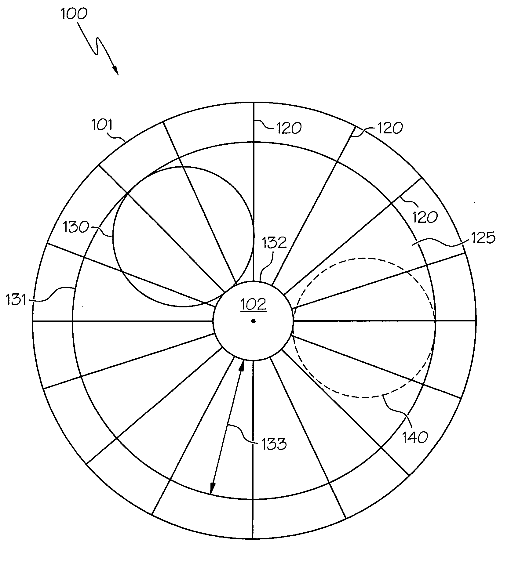
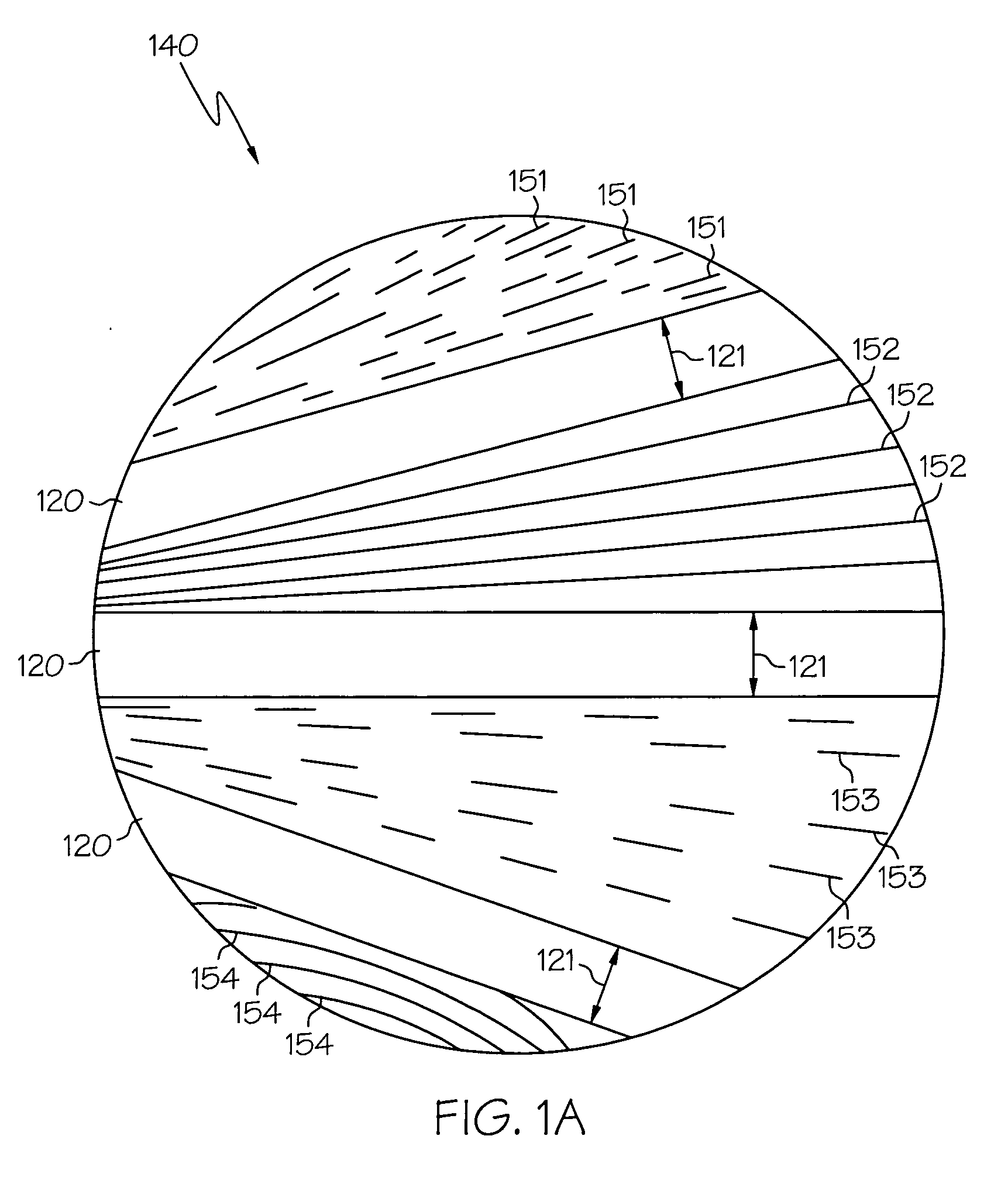
[0024] The invention relates to polishing pads having a macro- and micro-texture that reduces groove pattern transfer effects on the resulting polished substrate. It has been discovered that radial conditioning can reduce surface non-uniformities on magnetic, optical and semiconductor substrates. For purposes of this specification, radial direction refers to a path within 60 degrees of a straight line from the center to the circumference of the polishing pad (“radial direction”). Preferably, the micro-channels are within 45 degrees and most preferably within 30 degrees of the radial direction. The radial micro-channels produced by conditioning can facilitate outward slurry distribution that can reduce under-polished regions associated with the groove pattern transfer phenomena. Typically, the greater percentage of micro-channels with a radial direction, the less under-polished regions result from the polishing. For purposes of this specification, a majority of radial-biased micro-ch...


PUM

PropertyMeasurementUnit
Lengthaaaaaaaaaa
Angleaaaaaaaaaa
Areaaaaaaaaaaa

Abstract

The polishing pad is useful for polishing magnetic, optical and semiconductor substrates. The pad includes a polishing layer having a rotational center and an annular polishing track concentric with the rotational center and has a width. The width of the annular polishing track is free of non-radial grooves. And the pad has a plurality of radial micro-channels in the polishing layer within the width of the annular polishing track with a majority of the radial micro-channels having primarily a radial orientation and an average width less than 50 μm.

Description

CROSS REFERENCE TO RELATED APPLICATION [0001] This application claims the benefit of U.S. Provisional Application Ser. No. 60 / 670,466 filed Apr. 12, 2005.BACKGROUND OF THE INVENTION [0002] The present invention relates generally to the field of polishing pads for chemical mechanical polishing. In particular, the present invention relates to conditioned polishing pads useful for chemical mechanical polishing magnetic, optical and semiconductor substrates. [0003] In the fabrication of integrated circuits and other electronic devices, multiple layers of conducting, semiconducting and dielectric materials are deposited onto and removed from a surface of a semiconductor wafer. Thin layers of conducting, semiconducting and dielectric materials may be deposited using a number of deposition techniques. Common deposition techniques in modern wafer processing include physical vapor deposition (PVD), also known as sputtering, chemical vapor deposition (CVD), plasma-enhanced chemical vapor depo...

Claims


Application Information

Patent Timeline
IPC IPC(8): B24B1/00B24D11/00B24D99/00B24B37/26
CPCB24B37/26D21H27/001D21H27/20D21H27/36
Inventor MULDOWNEY, GREGORY P.
Owner ROHM & HAAS ELECTRONICS MATERIALS CMP HLDG INC
Why Eureka
Try Eureka