Magnetic memory device

a memory device and magnetic field technology, applied in the field of magnetic memory devices, can solve the problems of data recording errors, thermal unstability of the memory device, and affecting the stability of the magnetic field of the first, and achieve the effect of reducing the static magnetic field of the memory devi

Inactive Publication Date: 2006-11-09
AGENCY FOR SCI TECH & RES
View PDF6 Cites 7 Cited by
  • Summary
  • Abstract
  • Description
  • Claims
  • Application Information

AI Technical Summary

Benefits of technology

[0018] Preferably, the memory cell further comprises an anti-ferromagnetic layer disposed adjacent to one of the first and the second hard magnetic layers to fix the orientation of the magnetization vector therein. More preferably, the memory cell further comprises an assistant magnetic layer disposed adjacent to one of the first and the second hard magnetic layers, the assistant magnetic layer has a magnetization vector anti-parallelly aligned with one of the first and the second hard magnetic layers to reduce the static magnetic field thereof.

Problems solved by technology

One problem encountered in this type of memory cell is that the second magnetic layer 116 generates a static field and applies on the first magnetic layer 12, which tends to disrupt the stability of the magnetization of the first magnetic layer 112.
For example, when the dimensions of the memory cells shrink, external thermal fluctuations will cause the magnetization vector of the first magnetic layer 112 to rotate, which may cause data recording errors.
Another problem encountered in this type of memory cell is that with the size of the memory cells scaled down, there generates a large edge domain in the first magnetic layer 112, which also contributes to the thermal unstability of the memory device.
While the thermal stability may be increased in this type of memory device, another problem arises as since the synthetic ferromagnetic layers required a larger writing current to perform the writing operation, the power dissipation of this type of device increases.
In this structure, however, the large edge domain effect which contributes to the thermal instability of the device, remain unsolved.

Method used


Image

  • Magnetic memory device
  • Magnetic memory device
  • Magnetic memory device

Examples


Embodiment Construction

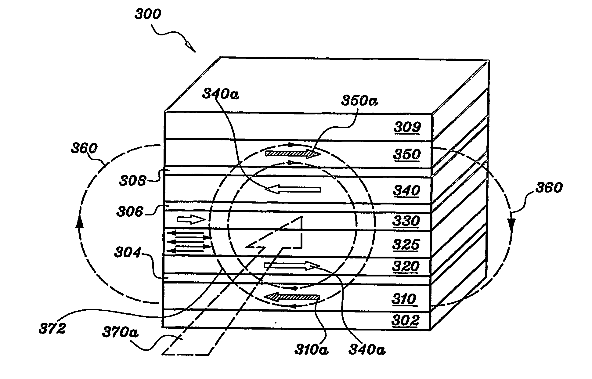
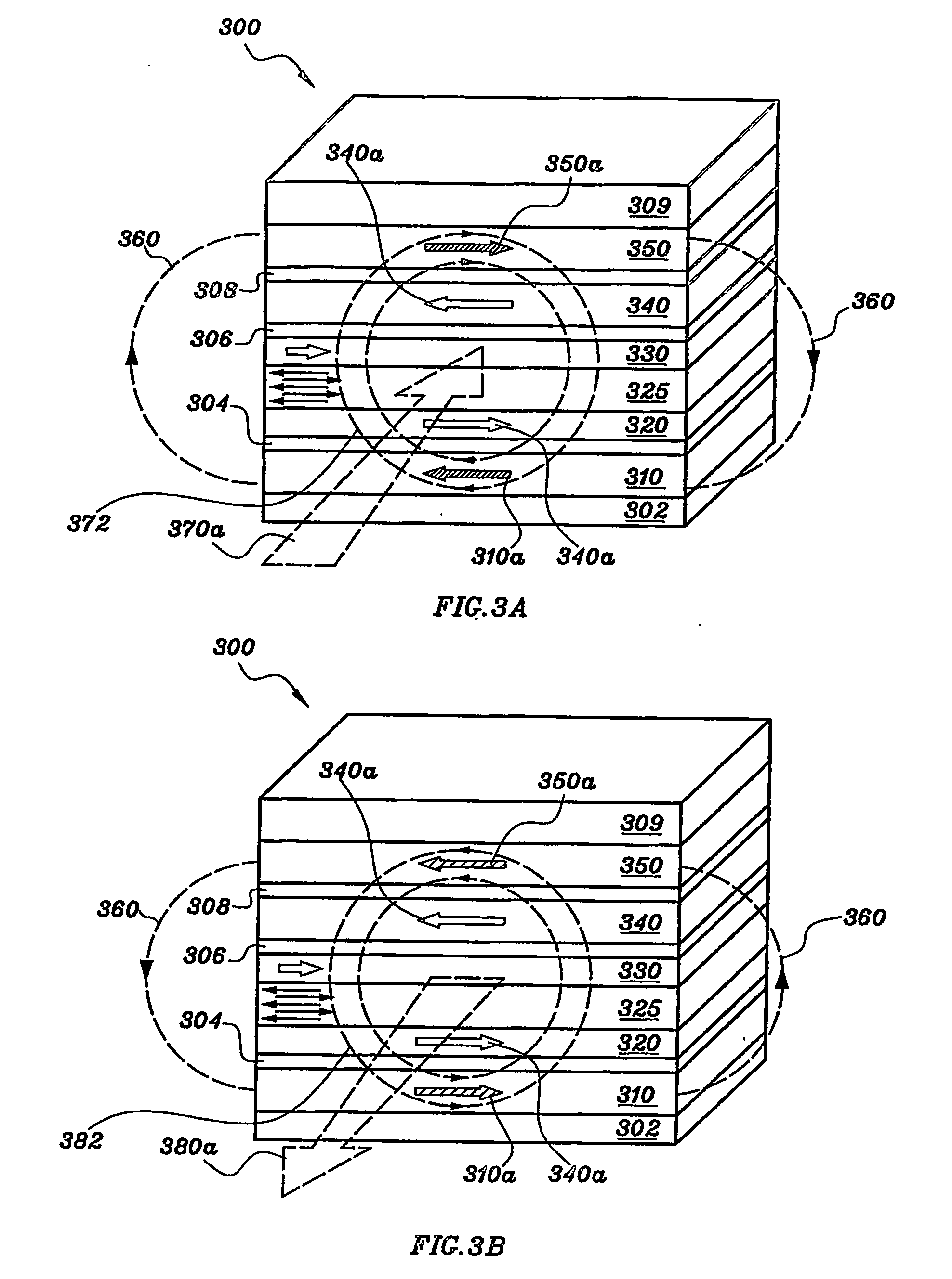
[0035] As shown in FIGS. 3A and 3B, a memory cell 300 for a magnetic memory device according to one embodiment of the present invention comprises a template layer 302, a first free layer 310, a first non-magnetic layer 304; a first ferromagnetic layer 320, an antiferromagnetic layer 325, a second ferromagnetic layer 330, a second non-magnetic layer 306, a third ferromagnetic layer 340, a third non-magnetic layer 308, a second free layer 350 and a cap layer 309. The above layers are disposed in sequence, and the first and third ferromagnetic layers 320 and 340 are disposed between the two free layers 310 and 350, as shown in FIG. 3A.

[0036] In this structure, the two ferromagnetic layers 320 and 340 serve as the pinned layer, and the two free layers 310 and 350 are the record layers with their initial magnetization anti-parallelly oriented. The two free layers 310 and 350 are magnetostatically coupled to each other to form a flux-closure 360.

[0037] In the embodiment shown in FIG. 3A...


PUM


Abstract

A memory cell for a magnetic memory device comprising a first hard magnetic later having a first fixed magnetization vector; a second hard magnetic later having a second fixed magnetization vector; a first soft magnetic layer having a first alterable magnetization vector and disposed adjacent to the first hard magnetic layer and a second soft magnetic layer having a second alterable magnetization vector and disposed adjacent to the second hard magnetic layer, the first and the second soft magnetic layers are magnetostatically coupled antiparallel to each other to form a flux-closed structure. An electrically conductive layer is disposed between the two soft magnetic layers for passing an electric current therethrough to perform the read and write operations. A magnetic memory device made thereof possesses a higher thermal stability against external thermal fluctuations and in the meantime has a lower power dissipation in writing operations.

Description

FIELD OF THE INVENTION [0001] The present invention relates to a magnetic memory device. In particular, it relates to a spin-valve magnetoresistive random access memory device. BACKGROUND OF THE INVENTION [0002] Magnetoresistive random access memory (MRAM) devices are solid state, non-volatile memory devices. A conventional MRAM device includes a column of first electrical wires (referred to as “word lines”) and a row of second electrical wires (referred to as “bit lines”). An array of magnetic memory cells are located at the junctions of the word lines and bit lines is used to record data signals. [0003] A typical MRAM cell comprises a hard magnetic layer, a soft magnetic layer and a non-magnetic layer sandwiched between the hard magnetic layer and the soft magnetic layer. The hard magnetic layer has its magnetization vector fixed in one direction. The orientation of the fixed magnetization vectors does not change under a magnetic field applied thereon. The soft magnetic layer has ...

Claims


Application Information

Patent Timeline
Patent Type & Authority Applications(United States)
IPC IPC(8): G11C11/14G11C11/15G11C11/16
CPCG11C11/16
Inventor ZHENG, YUANKAIWU, YIHONG
Owner AGENCY FOR SCI TECH & RES
Why Eureka
Try Eureka