Electrostatic discharge testing

a technology of electrostatic discharge and testing method, which is applied in the field of system and method of electrostatic discharge testing, can solve the problems of affecting the performance of the device, and affecting the quality of the device,

Inactive Publication Date: 2007-01-25
AVAGO TECH WIRELESS IP SINGAPORE PTE
View PDF13 Cites 19 Cited by
  • Summary
  • Abstract
  • Description
  • Claims
  • Application Information

AI Technical Summary

Benefits of technology

[0014] According to the system and method disclosed herein, the system provides on-c

Problems solved by technology

Electrostatic discharge (ESD) is a well-known problem.
ESD is a fast discharge of current that can damage semiconductor chips or devices.
Some devices may be more readily damaged by discharges occurring within automated equipment, while others may be more prone to damage from handling by personnel.
If ESD damage renders a device completely nonfunctional, the device is simply discarded.
However, ESD damage may be mild enough such that the ESD damage results in intermittent failures.
Intermittent failures are typically more problematic, because such damage may not become apparent until the device is already in the field.
Also, the performance of a damaged device may be compromised before the device actually malfunctions.
HBM is one of the most common causes of ESD dam

Method used


Image

  • Electrostatic discharge testing
  • Electrostatic discharge testing
  • Electrostatic discharge testing

Examples


Embodiment Construction

[0021] The present invention relates to semiconductor chips, and more particularly to a system for electrostatic discharge (ESD) testing. The following description is presented to enable one of ordinary skill in the art to make and use the invention, and is provided in the context of a patent application and its requirements. Various modifications to the preferred embodiment and the generic principles and features described herein will be readily apparent to those skilled in the art. Thus, the present invention is not intended to be limited to the embodiments shown, but is to be accorded the widest scope consistent with the principles and features described herein.

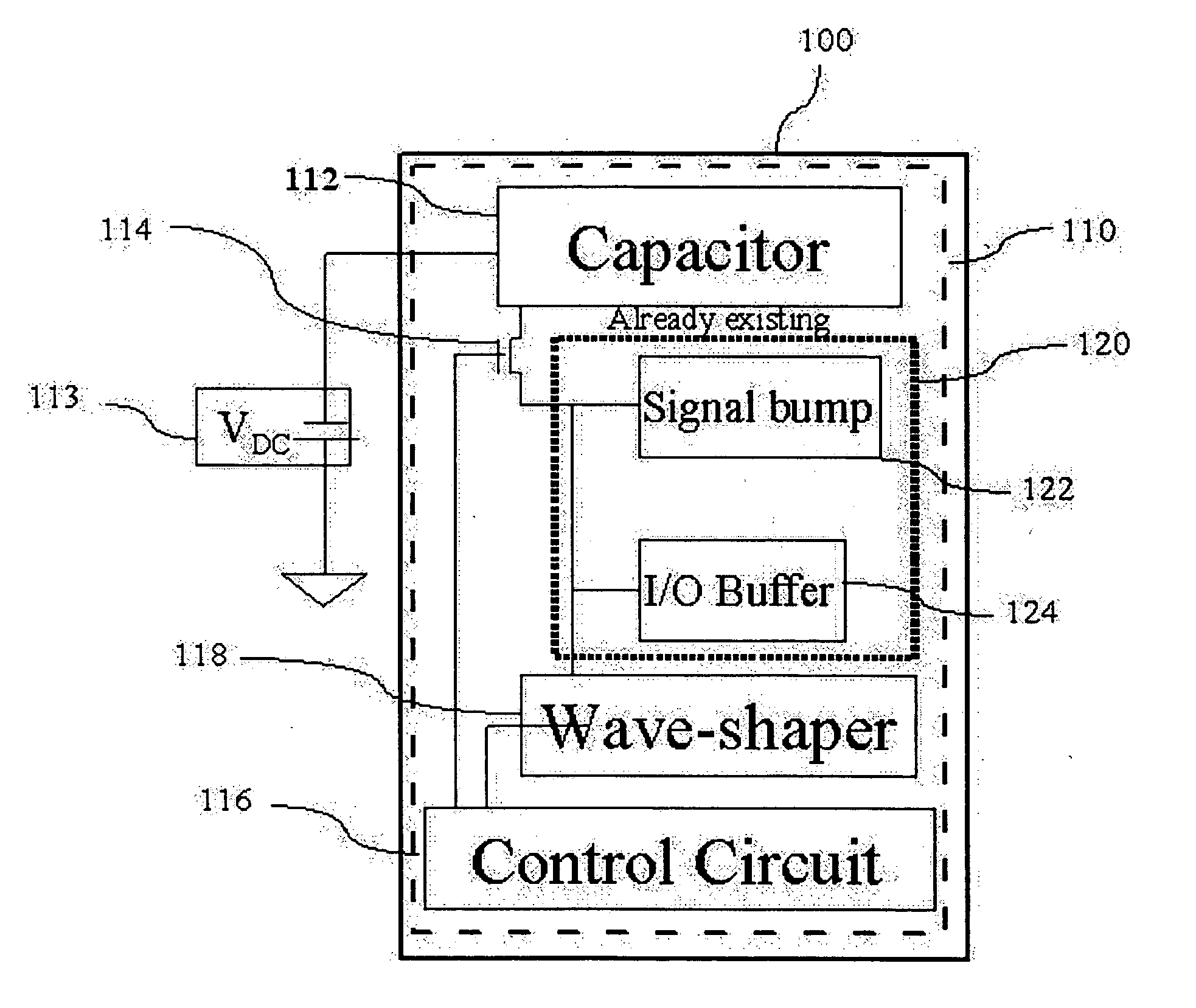
[0022] The preferred embodiment of the present invention provides a system for ESD testing that integrates an ESD tester into a device under test (DUT). The ESD tester includes a circuit that has a capacitor that is coupled to one or more input / output (I / O) circuits of the DUT via a switch that is controlled by a control ...


PUM


Abstract

The present invention provides a system and method for electrostatic discharge (ESD) testing. The system includes a circuit that has a switch coupled to an input/output (I/O) circuit of a device under test (DUT), a charge source coupled to the switch, and a control circuit coupled to the switch, wherein the control circuit turns on the switch to discharge an ESD current from the charge source to the I/O circuit, and wherein the circuit is integrated into the DUT. According to the system and method disclosed herein, the system provides on-chip ESD testing of a DUT without requiring expensive and specialized test equipment.

Description

FIELD OF THE INVENTION [0001] The present invention relates to semiconductor chips, and more particularly to a system and method for electrostatic discharge testing. BACKGROUND OF THE INVENTION [0002] Electrostatic discharge (ESD) is a well-known problem. ESD is a fast discharge of current that can damage semiconductor chips or devices. The degree of damage to a device by an ESD event is determined by the device's ability to dissipate the energy of the discharge or ability to withstand the current levels involved. Some devices may be more readily damaged by discharges occurring within automated equipment, while others may be more prone to damage from handling by personnel. [0003] If ESD damage renders a device completely nonfunctional, the device is simply discarded. However, ESD damage may be mild enough such that the ESD damage results in intermittent failures. Intermittent failures are typically more problematic, because such damage may not become apparent until the device is alr...

Claims


Application Information

Patent Timeline
IPC IPC(8): G01R31/26
CPCG01R31/002
Inventor ITO, CHOSHULOH, WILLIAM M.CHEN, JAU-WEN
Owner AVAGO TECH WIRELESS IP SINGAPORE PTE
Why Eureka
Try Eureka