High-density, robust connector for stacking applications

a stacking application, high-density technology, applied in the direction of coupling device connection, coupling protective earth/shielding arrangement, electrical equipment, etc., can solve the problem of increasing the size and cost adding additional cost in the manufacture and assembly of connectors, and large overall relative size of shielded backplane connectors. to achieve the effect of broadside coupling

Active Publication Date: 2007-01-25
MOLEX INC
View PDF30 Cites 76 Cited by
  • Summary
  • Abstract
  • Description
  • Claims
  • Application Information

AI Technical Summary

Benefits of technology

[0008] Another object of the present invention is to provide a connector for use in connecting circuits in two circuit boards together that has a high terminal density, high speed with low crosstalk and which is robust.
[0011] An additional object of the present invention is to provide a wafer connector component in which two columns of conductive terminals are supported in an insulative support body, the body including an internal cavity disposed between the two columns of conductive terminals, the terminal being arranged in horizontal pairs of terminal, the cavity defining an air channel between each horizontal pair of terminals arranged in the two columns of terminals, and the terminals being further aligned with each other in each row so that horizontal faces of the terminals in the two rows face each other to thereby promote broadside coupling between horizontal pairs of terminals.
[0012] Yet another object of the present invention is to provide a header connector for use in backplane applications, that is, connecting two circuit boards together, the connector including a cover member, or shroud, that is supportable on a circuit board, the cover member having a hollow interior defined by opposing side and end walls, the cover member receiving a plurality of terminal assemblies therein, each of the terminal assemblies extending lengthwise between two opposing side walls, and each of the terminal assemblies supporting two rows of conductive terminals, the rows of terminal being aligned with each other so that the terminals of one row of each of the terminal assemblies are able to capacitively couple in a broadside manner, with the terminals of the other row of the terminal assembly, the terminals including bifurcated contact portions and compliant pin tail portions.

Problems solved by technology

High speed signal transfer has in the past required the differential signal terminals to be shielded and this shielding increased the size and cost of backplane connectors because of the need to separately form individual shields that were assembled into the backplane connector.
The use of shields also added additional cost in the manufacture and assembly of the connectors and because of the width of the separate shield elements, the overall relative size of a shielded backplane connector was large.

Method used


Image

  • High-density, robust connector for stacking applications
  • High-density, robust connector for stacking applications
  • High-density, robust connector for stacking applications

Examples


Embodiment Construction

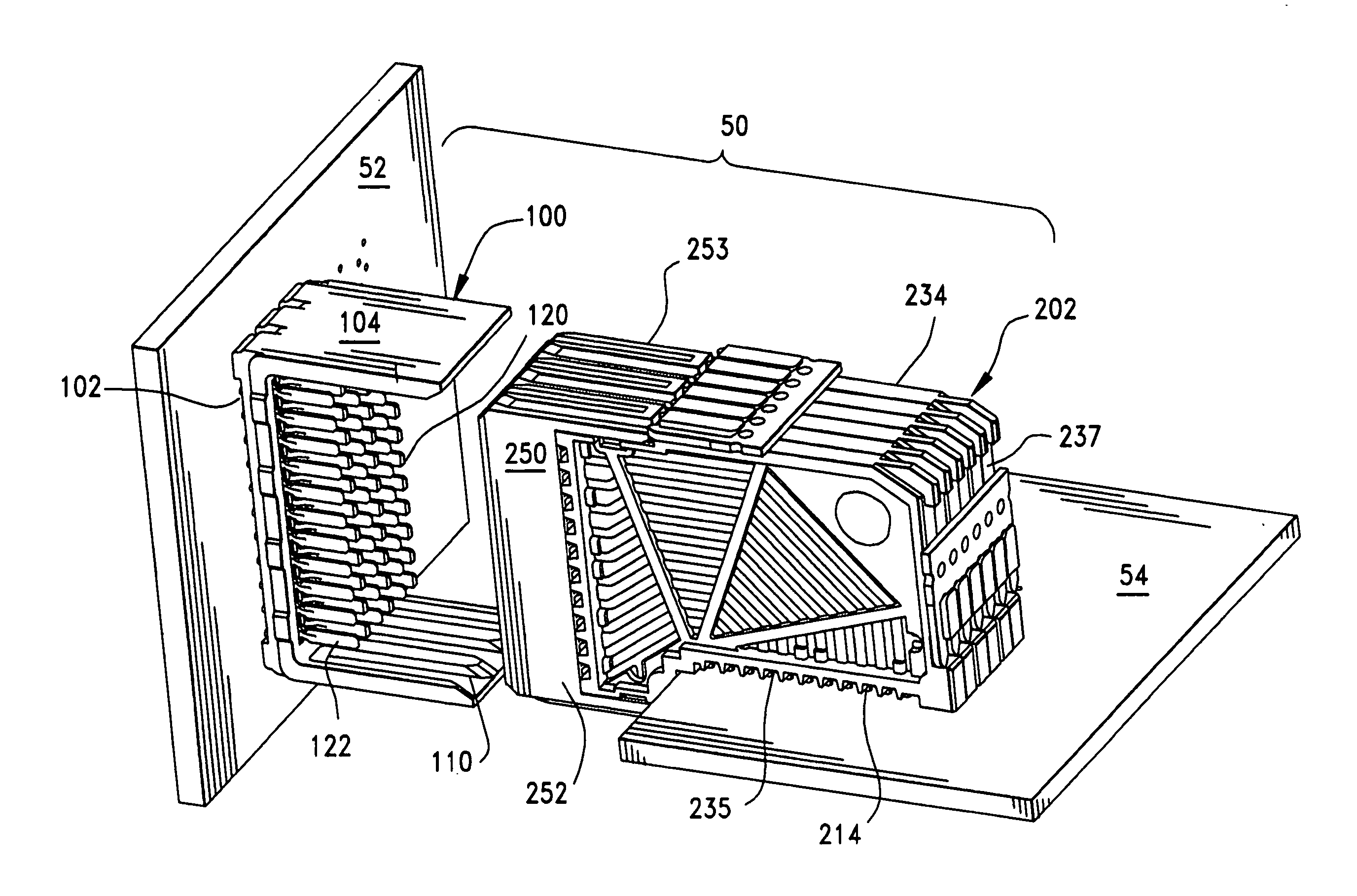
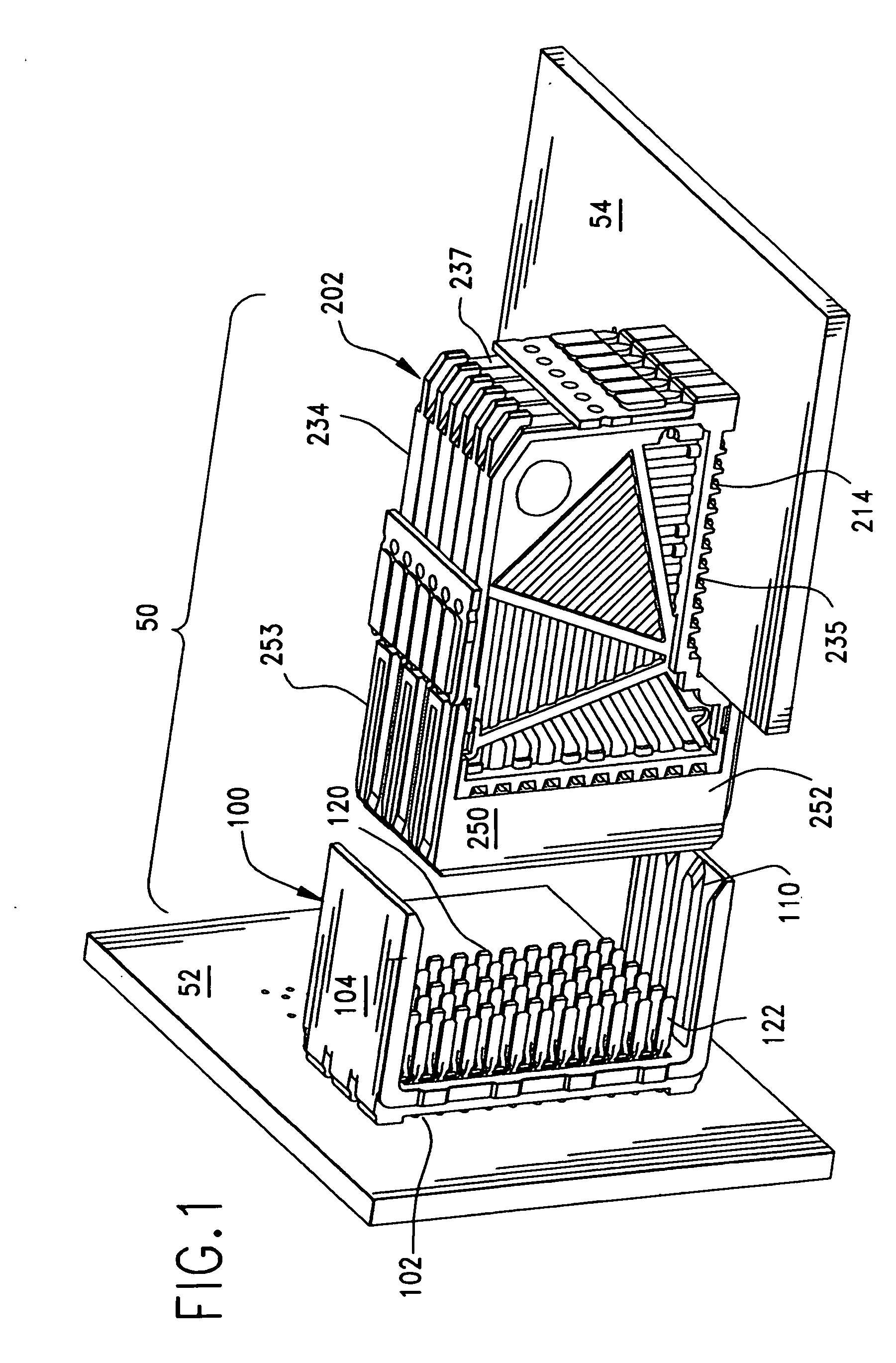
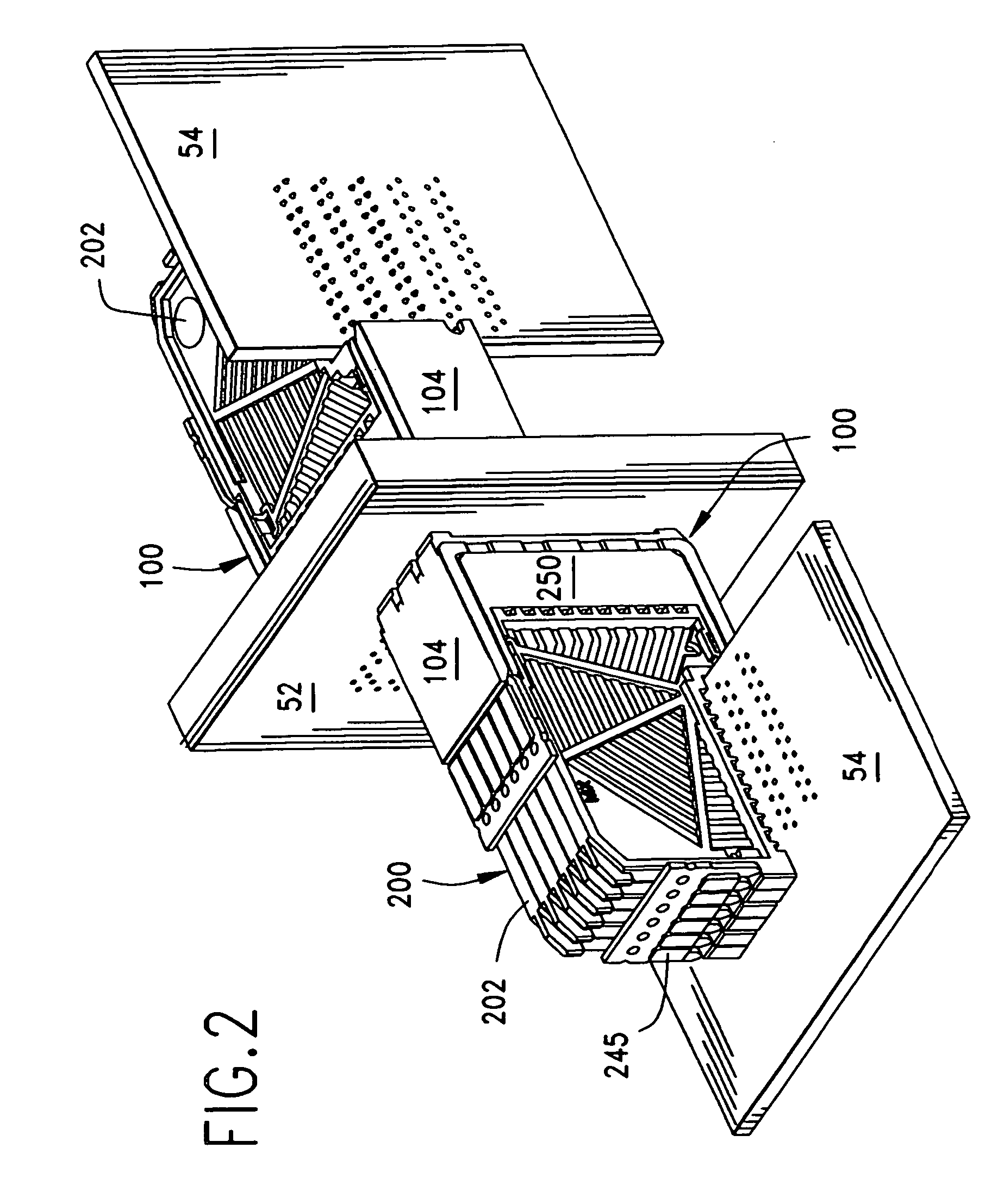
[0065]FIG. 1 illustrates a backplane connector assembly 50 constructed in accordance with the principles of the present invention. The assembly 50 is used to join together two circuit boards 52, 54 with the circuit board 52 representing a backplane and the circuit board 54 representing an ancillary, or daughter board.

[0066] The assembly 50 can be seen to include two interengaging, or mating, components 100 and 200. One component 100 is mounted to the backplane board 52 and is a backplane member that takes the form of a pin header. In this regard, the backplane member 100, as illustrated best in FIGS. 1 and 3, includes a base portion 102 with two sidewalls 104, 106 rising up from the base portion 102. These two sidewalls 104, 106 serve to define a series of channels, or slots 108, each slot of which receives a single wafer connector component 202. In order to facilitate the proper orientation of the wafer connector components 202 within the backplane connector component, the sidewal...


PUM


Abstract

A high speed connector includes a plurality of terminal assemblies in which two columns of conductive terminals are supported in an insulative support body, the body including an internal cavity disposed between the two columns of conductive terminals. The terminals are arranged in horizontal pairs, and the internal cavity defines an air channel between each horizontal pair of terminals arranged in the two columns of terminals. The terminals are further aligned with each other in each row so that horizontal faces of the terminals in the two rows face each other to thereby promote broadside coupling between horizontal pairs of terminals.

Description

REFERENCE TO RELATED APPLICATIONS [0001] This application claims priority of prior U.S. Provisional Patent Application No. 60 / 666,971, filed Mar. 31, 2005. BACKGROUND OF THE INVENTION [0002] The present invention pertains generally to electrical connectors, and more particularly to an improved connector suitable for use in backplane applications. [0003] Backplanes are large circuit boards that contain various electrical circuits and components. They are commonly used in servers and routers in the information and technology areas. Backplanes are typically connected to other backplanes or to other circuit boards, known as daughter boards, which contain circuitry and components. Data transfer speeds for backplanes have increased as backplane technology has advanced. A few years ago, data transfer speeds of 1 Gigabit per second (Gb / s) were considered fast. These speeds have increased to 3 Gb / s to 6 Gb / s and now the industry is expecting speeds of 12 Gb / s and the like to be implemented i...

Claims


Application Information

Patent Timeline
Patent Type & Authority Applications(United States)
IPC IPC(8): H01R13/648
CPCH01R13/514H01R13/518H01R12/737H01R12/712H01R12/724H01R12/727
Inventor LAURX, JOHN C.DUNHAM, DAVID E.ELO, TIMOTHY S.HUMBERT, GARY
Owner MOLEX INC
Why Eureka
Try Eureka