
High-density, robust connector with guide means

a connector and guide means technology, applied in the field of connectors, can solve the problems of increasing the size and cost increasing the cost of shielding in the manufacture and assembly of connectors, and large overall relative size of shielded backplane connectors, so as to prevent possible stubbing of contact parts and promote broadside coupling

Active Publication Date: 2007-01-25
MOLEX INC
View PDF26 Cites 52 Cited by
  • Summary
  • Abstract
  • Description
  • Claims
  • Application Information

AI Technical Summary

Benefits of technology

The present invention provides a new backplane connector for use in next generation backplane applications. The connector has a high terminal density, high speed with low crosstalk, and is robust. It includes a backplane header component and a wafer connector component that mate together. The backplane header has a plurality of conductive terminals with flat contact blades and compliant tails that are offset from each other and the cavities in the header have air channels between them to promote broadside coupling between terminals. The wafer connector component has conductive terminals arranged in two vertical columns with horizontal rows of terminals and an internal cavity with air channels between the columns for capacitive coupling. The contact portions of the terminals extend forwardly of the wafer and are formed as bifurcated contacts with a cantilevered contact beam structure. The invention also provides guide members for orienting the connectors and reducing stubbing.

Problems solved by technology

High speed signal transfer has in the past required the differential signal terminals to be shielded and this shielding increased the size and cost of backplane connectors because of the need to separately form individual shields that were assembled into the backplane connector.
The use of shields also added additional cost in the manufacture and assembly of the connectors and because of the width of the separate shield elements, the overall relative size of a shielded backplane connector was large.

Method used


Image

  • High-density, robust connector with guide means
  • High-density, robust connector with guide means
  • High-density, robust connector with guide means

Examples


Embodiment Construction

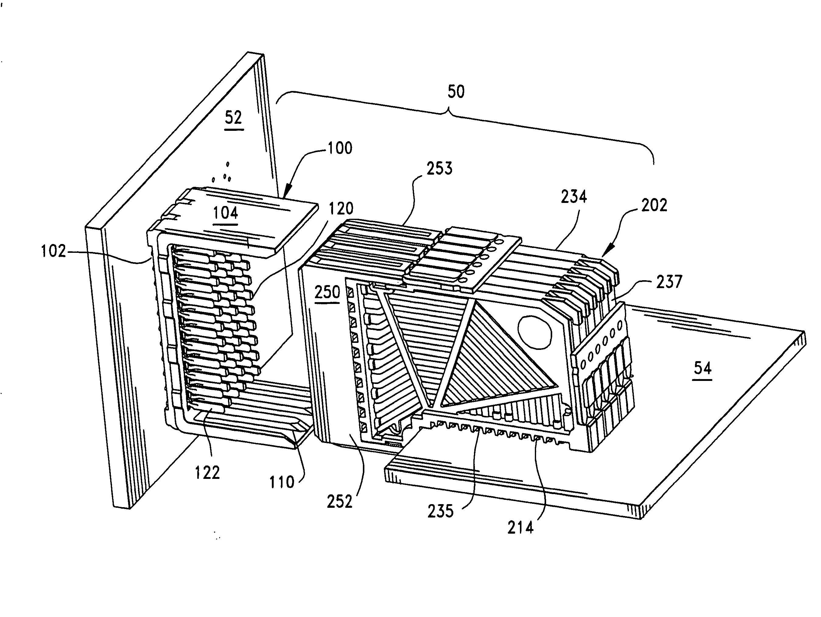
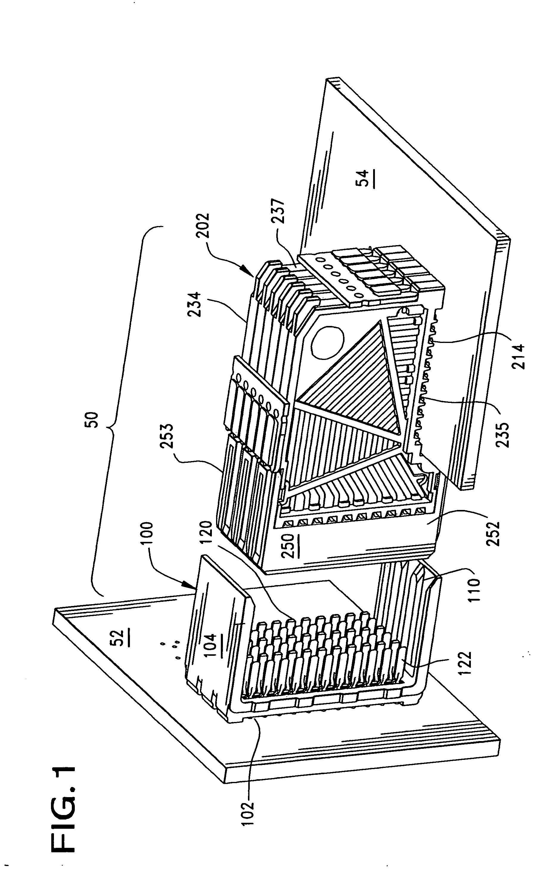
[0055]FIG. 1 illustrates a backplane connector assembly 50 constructed in accordance with the principles of the present invention. The assembly 50 is used to join together two circuit boards 52, 54 with the circuit board 52 representing a backplane and the circuit board 54 representing an ancillary, or daughter board.

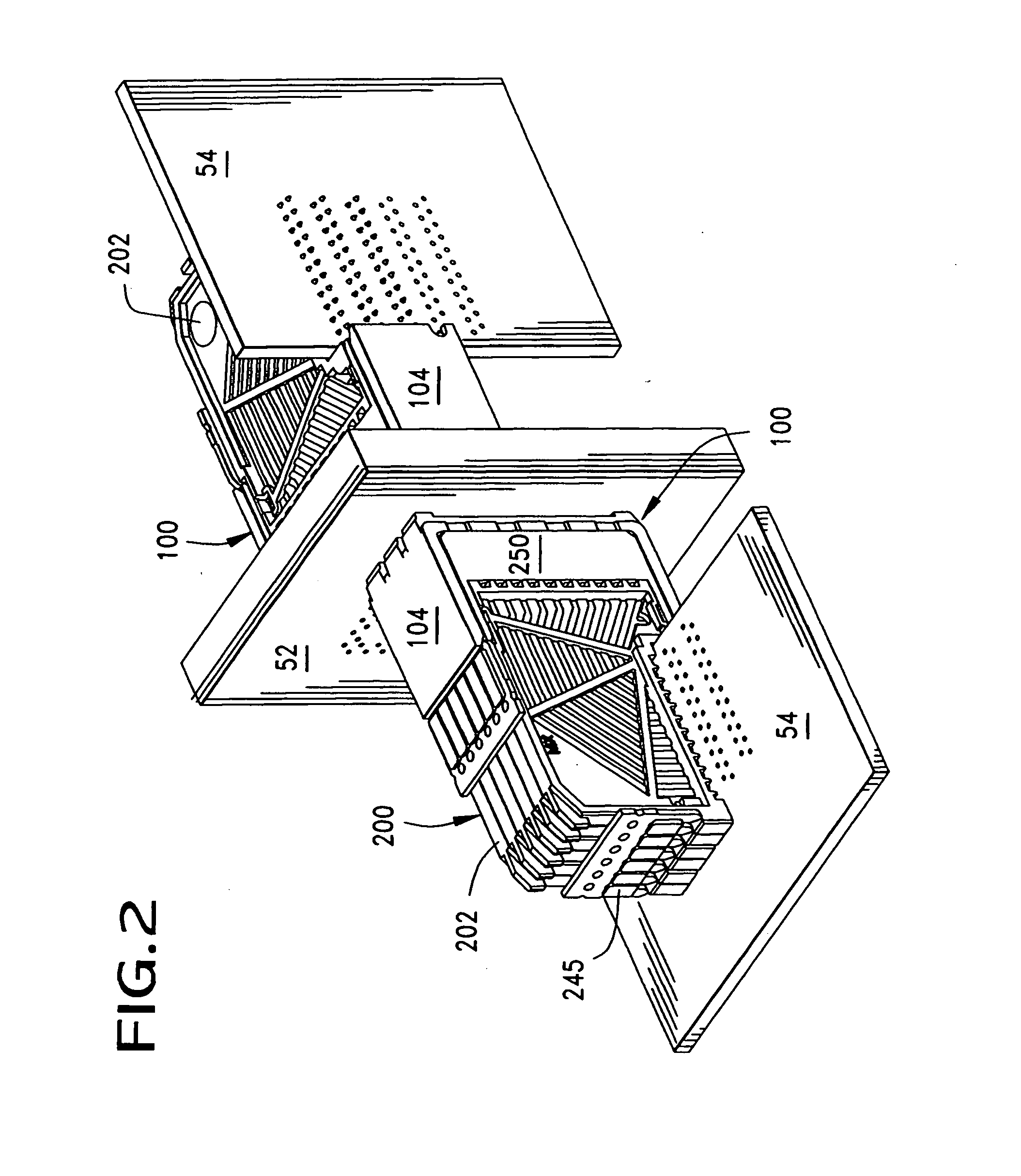
[0056] The assembly 50 can be seen to include two interengaging, or mating, components 100 and 200. One component 100 is mounted to the backplane board 52 and is a backplane member that takes the form of a pin header. In this regard, the backplane member 100, as illustrated best in FIGS. 1 and 3, includes a base portion 102 with two sidewalls 104, 106 rising up from the base portion 102. These two sidewalls 104, 106 serve to define a series of channels, or slots 108, each slot of which receives a single wafer connector component 202. In order to facilitate the proper orientation of the wafer connector components 202 within the backplane connector component, the sidewal...


PUM


Abstract

A high speed connector includes a plurality of wafer-style components in which two columns of conductive terminals are supported in an insulative support body, the body including an internal cavity disposed between the two columns of conductive terminals. The terminals are arranged in horizontal pairs, and the internal cavity defines an air channel between each horizontal pair of terminals arranged in the two columns of terminals. The terminals are further aligned with each other in each row so that horizontal faces of the terminals in the two rows face each other to thereby promote broadside coupling between horizontal pairs of terminals. Guide members are provided and are attached to the components to provide a means for guiding the components into engagement with opposing connectors.

Description

BACKGROUND OF THE INVENTION [0001] The present invention pertains generally to electrical connectors, and more particularly to an improved connector suitable for use in backplane applications. [0002] Backplanes are large circuit boards that contain various electrical circuits and components. They are commonly used in servers and routers in the information and technology areas. Backplanes are typically connected to other backplanes or to other circuit boards, known as daughter boards, which contain circuitry and components. Data transfer speeds for backplanes have increased as backplane technology has advanced. A few years ago, data transfer speeds of 1 Gigabit per second (Gb / s) were considered fast. These speeds have increased to 3 Gb / s to 6 Gb / s and now the industry is expecting speeds of 12 Gb / s and the like to be implemented in the next few years [0003] At high data transfer speeds, differential signaling is used and it is desirable to reduce the crosstalk and skew in such test s...

Claims


Application Information

Patent Timeline
Patent Type & Authority Applications(United States)
IPC IPC(8): H01R13/648
CPCH01R13/514H01R13/518H01R12/737H01R12/712H01R12/724H01R12/727
Inventor LAURX, JOHN C.
Owner MOLEX INC
Learn More