Thin film transistor substrate and method of making the same

a technology of thin film transistors and substrates, applied in the direction of semiconductor devices, instruments, electrical equipment, etc., can solve the problems of failure to planarize organic semiconductors, wall failure to retain water and oil repellency,

Active Publication Date: 2007-02-01
SAMSUNG DISPLAY CO LTD
View PDF7 Cites 95 Cited by
  • Summary
  • Abstract
  • Description
  • Claims
  • Application Information

AI Technical Summary

Problems solved by technology

However treating with CF4 plasma, which treats an inner part of the wall where the organic semiconductor is disposed as well as the wall, fails to planarize the organic semiconductor and the wall fails to retain water and oil repellency.

Method used


Image

  • Thin film transistor substrate and method of making the same
  • Thin film transistor substrate and method of making the same
  • Thin film transistor substrate and method of making the same

Examples


first embodiment

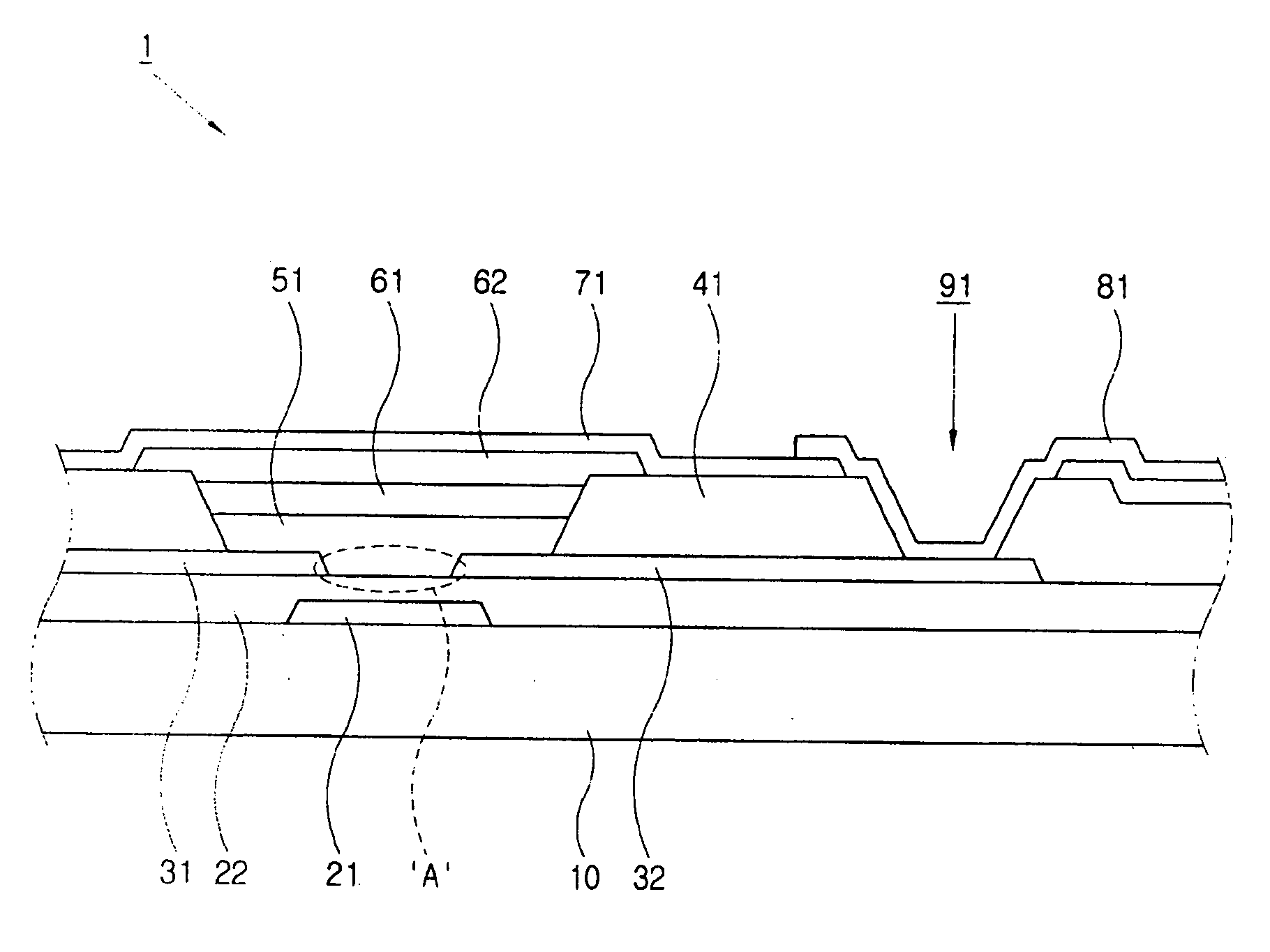
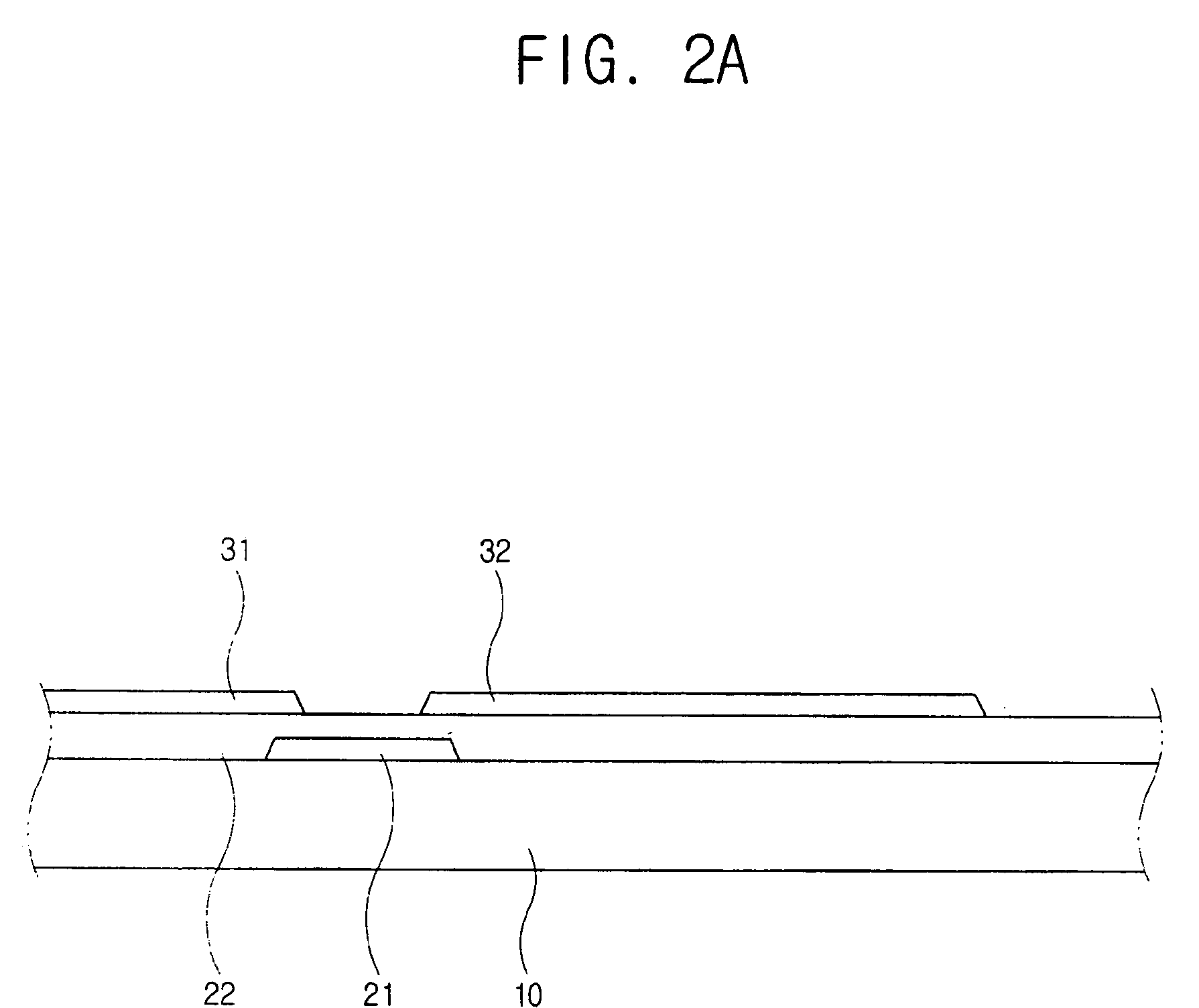
[0009]FIG. 1 is a sectional view of a TFT substrate according to the present invention. A TFT substrate 1 includes an insulating substrate 10, a source electrode 31 and a drain electrode 32 which are formed on the insulating substrate 10 and separated from each other, a wall 41 exposing a portion of the source electrode 31 and a portion of the drain electrode 32, and an organic semiconductor layer 51 disposed in the wall 41. The insulating substrate 10 is made of glass or plastic. When the insulating layer 10 is made of plastic, the TFT substrate 1 is flexible but is vulnerable to heat. The organic semiconductor layer 51 may be made of plastic because of being formed at normal temperature and pressure. The plastic may be polycarbon, polyimide, polyethersulfone (PES), polyarylate (PAR), polyethylenenaphthalate (PEN), and polyethyleneterephthalate (PET).

[0010] A light shield layer 21 is formed on the insulating substrate 10 and an insulating layer 22 is formed on the light shield laye...

third embodiment

[0032] As shown in FIG. 4, a wall 41 encompasses a channel area and is not disposed below the pixel electrode 81 in a TFT substrate 1 according to a Accordingly, the only passivation layer 71 is removed where the drain contact hole 91, exposing a drain electrode 32, is disposed.

fourth embodiment

[0033] As shown in FIG. 5, a source electrode 31 and a drain electrode 32 are made of ITO or IZO, wherein the drain electrode 32 is formed in a single body with a pixel electrode 81 in a TFT substrate 1 according to a Furthermore, a wall 41 and a passivation layer 71 are not formed on the pixel electrode 81 to prevent brightness decreasing.

[0034] As shown in FIG. 6, a TFT substrate 1 according to a fifth embodiment is formed in a bottom-gate type the way a gate electrode 62 is disposed below an organic semiconductor layer 51, in a different way of the first embodiment. A metal shielding pattern 21 is not formed since the gate electrode 62 intercepts light incident from a lower part of an insulating substrate 10. A gate insulating layer 63 is disposed between the gate electrode 62 and the organic semiconductor layer 51. The gate insulating layer 63 may be an organic layer, an inorganic layer, or a double layer of an organic layer and an inorganic layer. According to the fifth embodi...


PUM


Abstract

The present invention relates to a thin film transistor substrate comprising: an insulating substrate; a source electrode and a drain electrode which are formed on the insulating substrate and separated from each other and have a channel area therebetween; a wall exposing at least portions of the source electrode and the drain electrode, respectively, encompassing the channel area, and formed of fluoropolymer; and an organic semiconductor layer formed inside the wall. Thus, the present invention provides a TFT substrate where an organic semiconductor layer is planarized. Further, the present invention also provides a method of making a TFT substrate of which an organic semiconductor layer is planarized.

Description

CROSS-REFERENCE TO RELATED APPLICATIONS [0001] This application claims the benefit of Korean Patent Application No. 2005-0068553, filed on Jul. 27, 2005, in the Korean Intellectual Property Office, which is hereby incorporated by reference for all purposes as if fully set forth herein. FIELD OF THE INVENTION [0002] The present invention relates to a thin film transistor substrate in which a wall is formed of fluoropolymer to planarize an organic semiconductor layer. DESCRIPTION OF THE RELATED ART [0003] A liquid crystal display (LCD) includes an LCD panel comprising a thin film transistor (TFT) substrate where TFTs are formed, a color filter substrate where color filter layers are formed, and a liquid crystal layer interposed between both substrates. The LCD panel does not emit light by itself, therefore a backlight unit is disposed in a rear of the TFT substrate to provide light. Transmittance of light is controlled according to alignment of the liquid crystal layer. The TFT includ...

Claims


Application Information

Patent Timeline
Patent Type & Authority Applications(United States)
IPC IPC(8): H01L27/12
CPCH01L51/0005H01L51/0545H01L51/0541H01L51/0097H10K71/135H10K10/464H10K10/466H10K77/111G02F1/136
Inventor LEE, YONG-UKOH, JOON-HAKKIM, BO-SUNGHONG, MUN-PYO
Owner SAMSUNG DISPLAY CO LTD
Why Eureka
Try Eureka